
With the rapid development of wireless communication, automotive radar, satellite communication, high-speed data transmission, and microwave electronic systems, PCB technology is facing increasingly demanding requirements for signal transmission performance.
Traditional FR-4 materials, while widely used in general electronic products, may not provide sufficient performance for high-frequency applications due to limitations in:
- Dielectric loss
- Signal attenuation
- Dielectric constant stability
- Thermal performance
For RF, microwave, and high-speed electronic systems, selecting the appropriate high-frequency PCB material and adopting suitable manufacturing processes are critical factors affecting:
- Signal integrity
- Impedance control
- Transmission efficiency
- Product reliability
This article introduces the key considerations for high-frequency PCB material selection, common high-frequency materials, and important manufacturing and processing methods.
1. What Is a High-Frequency PCB?
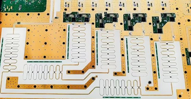
A high-frequency PCB is a circuit board designed to transmit electrical signals operating at high frequencies, typically above several hundred MHz and into the GHz range.
Compared with conventional PCBs, high-frequency PCBs require stricter control of:
- Dielectric properties
- Copper surface characteristics
- Layer structure
- Manufacturing precision
Typical applications include:
- RF communication equipment
- Microwave circuits
- 5G infrastructure
- Automotive radar systems
- Satellite communication
- High-speed computing equipment
2. Key Factors in High-Frequency PCB Material Selection
Material selection directly determines the electrical and mechanical performance of high-frequency PCBs.
Important parameters include:
2.1 Dielectric Constant (Dk)
The dielectric constant (Dk) affects:
- Signal propagation speed
- Trace impedance
- Wavelength characteristics
For high-frequency circuits, stable Dk is essential because variations can cause:
- Impedance deviation
- Phase errors
- Signal distortion
A low and stable dielectric constant helps improve signal transmission accuracy.
2.2 Dissipation Factor (Df)
The dissipation factor represents dielectric loss.
A lower Df means:
- Less energy loss
- Lower signal attenuation
- Better transmission efficiency
For microwave and high-frequency applications, low-loss materials are preferred.
2.3 Thermal Stability
High-frequency systems often operate under continuous electrical stress.
Material evaluation should consider:
- Glass transition temperature (Tg)
- Thermal expansion coefficient (CTE)
- Thermal conductivity
Good thermal stability improves:
- Reliability
- Dimensional accuracy
- Long-term performance
2.4 Moisture Absorption
Moisture can affect:
- Dielectric properties
- Signal performance
- Insulation reliability
High-frequency materials usually require low moisture absorption to maintain stable electrical characteristics.
2.5 Mechanical Properties
Material selection should also consider:
- Dimensional stability
- Layer bonding strength
- Processing compatibility
These factors affect:
- Multilayer fabrication
- Drilling quality
- Assembly reliability
3. Common High-Frequency PCB Materials
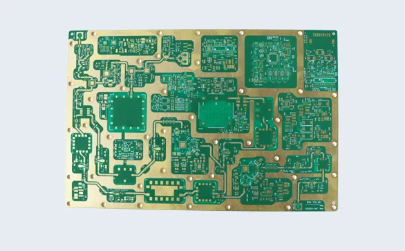
3.1 Rogers High-Frequency Laminates
Rogers materials are widely used in RF and microwave PCB applications.
Common materials include:
Rogers RO4003C
Characteristics:
- Low dielectric loss
- Stable electrical performance
- Good dimensional stability
Applications:
- RF modules
- Microwave circuits
- Communication equipment
Rogers RO4350B
Characteristics:
- Low-loss performance
- High thermal reliability
- Compatible with standard PCB processing
Applications:
- Power amplifiers
- RF front-end modules
- Automotive radar
Rogers RT/duroid Series
Characteristics:
- Excellent microwave performance
- Very low loss
Applications:
- Aerospace systems
- Satellite communication
- Precision microwave circuits
3.2 PTFE-Based Materials
PTFE materials are widely used for demanding microwave applications.
Advantages:
- Extremely low dielectric loss
- Excellent high-frequency stability
Challenges:
- Difficult processing
- Higher manufacturing requirements
Applications:
- Radar systems
- Microwave antennas
- High-frequency communication
3.3 Ceramic-Filled Materials
Ceramic-filled laminates provide:
- Stable dielectric properties
- Improved thermal performance
Applications:
- RF modules
- High-frequency circuits
- Power electronics
3.4 High-Performance FR-4 Materials
Advanced FR-4 materials can be used for moderate high-speed applications.
Advantages:
- Lower cost
- Mature processing
Applications:
- Digital communication boards
- High-speed control systems
4. Comparison of Common High-Frequency PCB Materials
| Material | Main Advantages | Typical Applications |
|---|---|---|
| FR-4 High Tg | Cost-effective, mature process | High-speed digital circuits |
| Rogers RO4003C | Low loss, stable Dk | RF and microwave circuits |
| Rogers RO4350B | Balanced electrical and thermal performance | RF modules, radar |
| PTFE | Extremely low loss | Advanced microwave systems |
| Ceramic PCB | High thermal conductivity | Power and RF applications |
5. High-Frequency PCB Production and Processing Methods
High-frequency PCB manufacturing requires stricter process control compared with standard PCB fabrication.
5.1 Material Preparation and Handling
High-frequency materials require careful handling due to sensitivity to:
- Temperature
- Humidity
- Mechanical stress
Proper storage conditions help maintain:
- Dielectric stability
- Material consistency
5.2 Stack-Up Design and Lamination
Stack-up design is one of the most important steps.
Engineers need to consider:
- Material thickness
- Dielectric spacing
- Copper thickness
- Signal layer arrangement
A proper stack-up helps achieve:
- Controlled impedance
- Reduced signal loss
- Better EMI performance
During lamination, manufacturers must control:
- Temperature
- Pressure
- Heating cycle
to prevent:
- Delamination
- Resin voids
- Layer shifting
5.3 Precision Drilling
High-frequency PCB drilling requires high accuracy.
Important considerations:
- Hole position accuracy
- Via reliability
- Surface quality
Poor drilling quality may cause:
- Signal discontinuity
- Impedance variation
- Reliability issues
5.4 Copper Surface Treatment
Copper surface roughness directly affects high-frequency signal loss.
At high frequencies, signals tend to travel along the conductor surface due to the skin effect.
Excessive copper roughness can increase:
- Insertion loss
- Transmission attenuation
Therefore, controlled copper treatment is important for high-performance RF boards.
5.5 Controlled Impedance Manufacturing
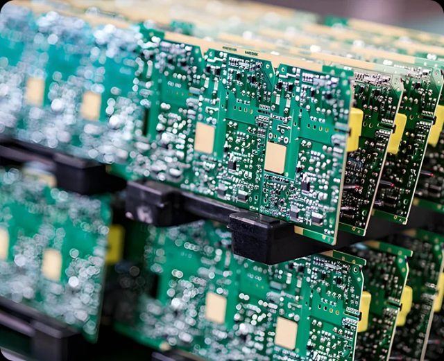
High-frequency PCB production requires impedance control throughout manufacturing.
Key factors include:
- Trace width
- Dielectric thickness
- Material Dk
- Copper thickness
Common impedance requirements:
- 50Ω single-ended impedance
- 90Ω/100Ω differential impedance
Verification methods include:
- TDR testing
- Impedance coupons
5.6 Surface Finish Selection
Surface finish affects:
- Signal transmission
- Assembly reliability
Common finishes include:
ENIG
Advantages:
- Flat surface
- Good solderability
- Suitable for fine-pitch components
ENEPIG
Advantages:
- Improved wire bonding compatibility
- Higher reliability
Suitable for:
- RF modules
- Advanced electronic packaging
6. High-Frequency PCB Design Considerations
6.1 Controlled Transmission Lines
High-frequency signals should use controlled structures such as:
- Microstrip lines
- Stripline structures
Design parameters include:
- Trace width
- Reference plane distance
- Dielectric properties
6.2 Grounding Design
A good grounding structure helps:
- Reduce noise
- Improve return paths
- Control EMI
Recommended practices:
- Use continuous ground planes
- Avoid unnecessary layer transitions
- Minimize return path discontinuity
6.3 Signal Integrity Analysis
Simulation and verification help identify:
- Reflection problems
- Crosstalk
- Signal attenuation
Common analysis methods:
- Electromagnetic simulation
- SI simulation
- Field solver analysis
7. Applications of High-Frequency PCBs
Communication Systems
Applications:
- 5G base stations
- Wireless modules
- RF transceivers
Requirements:
- Low signal loss
- Stable impedance
Automotive Radar
Applications:
- 24GHz radar
- 77GHz radar
Requirements:
- High-frequency stability
- Environmental reliability
Aerospace and Defense Electronics
Applications:
- Radar systems
- Satellite communication
Requirements:
- Extreme reliability
- Low-loss transmission
Industrial and Medical Equipment
Applications:
- Sensors
- Imaging systems
- Measurement devices
Requirements:
- Signal accuracy
- Stable operation
8. Challenges in High-Frequency PCB Manufacturing
High-frequency PCB production requires advanced manufacturing capabilities.
Common challenges include:
Material Processing
Different materials have different:
- Thermal expansion characteristics
- Lamination requirements
Impedance Variation Control
Small variations in:
- Copper thickness
- Dielectric thickness
- Trace dimensions
can affect performance.
Cost Control
High-frequency materials are generally more expensive than standard PCB materials.
Engineers need to balance:
- Performance requirements
- Manufacturing cost
- Product lifetime
Conclusion
High-frequency PCB performance depends on both proper material selection and precise manufacturing processes.
Selecting suitable materials such as:
- Rogers RO4003C
- Rogers RO4350B
- PTFE-based laminates
- Ceramic-filled materials
can significantly improve:
- Signal integrity
- Transmission efficiency
- Product reliability
At the same time, advanced manufacturing processes including:
- Controlled lamination
- Precision drilling
- Impedance control
- Copper surface optimization
are essential to achieve stable high-frequency performance.
As communication systems, radar technology, and high-speed electronics continue to evolve, high-frequency PCB materials and manufacturing technologies will remain critical factors supporting next-generation electronic products.
