
With the rapid development of wireless communication, radar systems, satellite communication, automotive electronics, and high-speed RF applications, traditional PCB technologies face increasing challenges in maintaining signal integrity and electrical performance at high frequencies.
High-frequency PCBs designed for microwave circuits require more than conventional circuit fabrication capabilities. Factors such as material characteristics, dielectric stability, impedance control, transmission loss, thermal performance, and manufacturing precision directly affect the final RF performance.
Unlike low-frequency digital circuits, microwave circuits are highly sensitive to small variations in PCB structure. Even minor changes in dielectric thickness, copper roughness, or trace geometry can influence insertion loss, phase stability, return loss, and overall system reliability.
Therefore, high-frequency PCB design requires a comprehensive approach combining RF engineering principles, material selection, simulation analysis, and manufacturing process control.
1. Understanding the Requirements of Microwave PCB Design
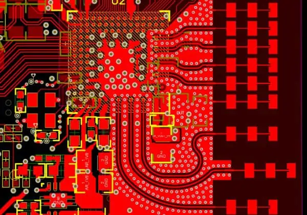
Microwave circuits typically operate in frequency ranges from several hundred MHz to GHz levels, where electromagnetic effects become dominant.
At high frequencies, PCB traces are no longer simple electrical connections. They behave as transmission lines, and their characteristics directly influence signal transmission.
Key performance requirements include:
- Low dielectric loss
- Stable dielectric constant (Dk)
- Controlled impedance
- Low signal attenuation
- Excellent thermal stability
- Reliable manufacturing consistency
A successful microwave PCB design must balance electrical performance with manufacturability and cost considerations.
2. Selecting Suitable High-Frequency PCB Materials
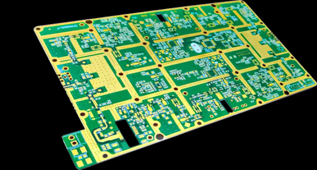
Material selection is one of the most critical steps in microwave PCB development.
Unlike standard FR-4 materials, which may have higher dielectric loss at high frequencies, RF applications typically require specialized low-loss laminates.
Common high-frequency PCB materials include:
PTFE-Based Materials
PTFE-based laminates are widely used in microwave applications due to their:
- Low dielectric loss
- Excellent high-frequency performance
- Stable electrical characteristics
They are commonly applied in:
- RF modules
- Antenna systems
- Radar equipment
- Microwave communication devices
However, PTFE materials require specialized processing due to their unique mechanical properties.
Rogers High-Frequency Materials
Materials such as Rogers RO3003™, RO4350B™, and RT/duroid™ series are commonly selected for RF and microwave PCB designs.
Advantages include:
- Controlled dielectric properties
- Low insertion loss
- Good thermal reliability
- Consistent performance at high frequencies
The appropriate material depends on frequency range, mechanical requirements, and application environment.
3. Importance of Controlled Impedance Design
In microwave circuits, impedance matching is essential for maintaining signal quality.
Poor impedance control can result in:
- Signal reflection
- Increased insertion loss
- Reduced transmission efficiency
- RF performance degradation
Common controlled impedance structures include:
- Microstrip lines
- Stripline structures
- Coplanar waveguides
During PCB design, engineers need to consider:
- Trace width
- Copper thickness
- Dielectric thickness
- Material dielectric constant
- Layer stack-up configuration
Accurate impedance simulation and manufacturing verification are necessary to ensure the designed electrical characteristics are achieved.
4. Managing Signal Loss in High-Frequency PCB Design
Signal loss becomes a major concern as frequency increases.
The main sources of loss include:
Dielectric Loss
Dielectric loss occurs when energy is absorbed by the PCB substrate material.
Materials with lower dissipation factor (Df) help reduce signal attenuation.
Copper Loss
At high frequencies, current tends to flow near the conductor surface, known as the skin effect.
Copper surface roughness can increase conductor loss, affecting:
- Insertion loss
- Phase response
- Signal integrity
Therefore, selecting suitable copper foil and surface treatment becomes important for microwave PCB performance.
5. PCB Stack-Up Design for Microwave Applications
A well-designed stack-up is essential for high-frequency performance.
Key considerations include:
Dedicated Signal Layers
High-frequency signal layers should be carefully arranged to minimize interference and maintain consistent impedance.
Ground Plane Optimization
A continuous ground reference helps:
- Reduce EMI
- Improve return current paths
- Enhance signal stability
Layer Symmetry
Balanced stack-up structures help reduce:
- PCB warpage
- Mechanical stress
- Manufacturing variation
Especially for multilayer RF boards, stack-up design should be reviewed before fabrication.
6. Thermal Management in High-Frequency Circuits
Microwave circuits often involve power amplifiers, transmit modules, and high-power RF components.
Excessive heat can affect:
- Frequency stability
- Material properties
- Component lifetime
- System reliability
Thermal design considerations include:
- Copper thickness optimization
- Thermal via structures
- Heat dissipation paths
- Material selection
A reliable high-frequency PCB must maintain stable electrical performance under operating temperature variations.
7. Manufacturing Challenges of Microwave PCBs
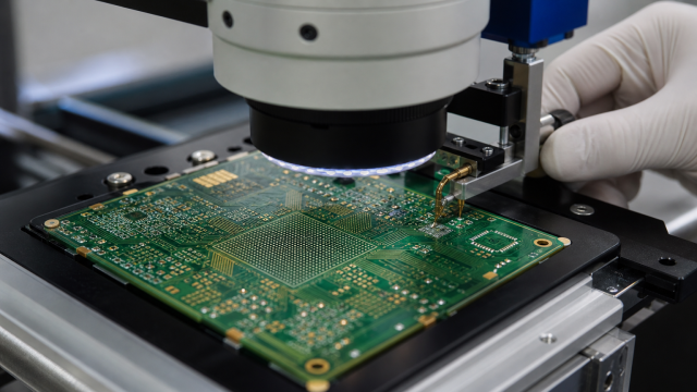
High-frequency PCB fabrication requires strict process control.
Important manufacturing factors include:
Material Processing
RF laminates may require special handling during:
- Drilling
- Lamination
- Plating
- Routing
Improper processing can affect dielectric consistency and signal performance.
Dimensional Accuracy
At microwave frequencies, small manufacturing deviations can influence impedance performance.
Critical parameters include:
- Trace width tolerance
- Dielectric thickness variation
- Layer alignment accuracy
- Copper thickness control
Testing and Verification
RF PCB quality verification may include:
- Impedance testing
- TDR analysis
- Insertion loss measurement
- Electrical testing
- Material verification
These processes help ensure the manufactured PCB matches the original RF design requirements.
8. Simulation and Design Verification Before Production
Before PCB fabrication, simulation tools are often used to evaluate RF performance.
Common analysis includes:
- Electromagnetic simulation
- Signal integrity analysis
- Impedance calculation
- Thermal simulation
Early design verification helps identify potential issues such as:
- Signal reflection
- Crosstalk
- Excessive loss
- Resonance problems
This reduces development risks and improves first-pass production success.
Conclusion
Designing a high-frequency PCB for microwave circuits requires a combination of advanced material knowledge, RF design principles, precise manufacturing capabilities, and strict quality control.
From selecting low-loss PCB materials and optimizing stack-up structures to controlling impedance and minimizing signal loss, every design detail can influence microwave performance.
As applications such as 5G communication, automotive radar, satellite systems, and advanced RF equipment continue to expand, high-frequency PCB technology will remain a key foundation for reliable microwave circuit development.
Through professional engineering support, material expertise, and manufacturing process control, PCB manufacturers can help customers transform complex RF designs into stable and production-ready solutions.
