
With the rapid development of wireless communication, radar systems, IoT devices, automotive electronics, and high-speed electronic products, RF (Radio Frequency) circuit design has become increasingly important. Compared with conventional PCB designs, RF PCB design involves more complex challenges related to signal integrity, impedance control, electromagnetic interference (EMI), and material selection.
At high frequencies, even small variations in PCB geometry, dielectric properties, or routing structures can significantly affect signal performance. Therefore, successful RF circuit and PCB layout design requires a comprehensive understanding of both electrical principles and manufacturing limitations.
This article introduces key considerations for designing reliable RF circuits and PCB layouts, helping engineers improve performance, stability, and manufacturability.
1. Understand RF Signal Characteristics Before Design
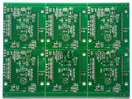
RF signals typically operate from hundreds of MHz to several GHz or even higher frequency ranges. At these frequencies, PCB traces are no longer simple conductors; they behave as transmission lines where impedance, electromagnetic fields, and signal propagation characteristics directly influence performance.
Key RF design factors include:
- Signal frequency and wavelength
- Characteristic impedance
- Insertion loss and return loss
- Crosstalk between RF traces
- Electromagnetic radiation
- Phase stability
Unlike low-frequency digital circuits, RF circuits are highly sensitive to discontinuities. A small impedance mismatch caused by an incorrect trace width, connector transition, or layer change can result in signal reflection and power loss.
2. Select Appropriate PCB Materials for RF Applications
PCB material selection is one of the most important decisions in RF design.
Traditional FR-4 materials may be suitable for low-frequency applications, but their dielectric properties can vary significantly at higher frequencies.
Important RF PCB material parameters include:
Dielectric Constant (Dk)
The dielectric constant affects signal propagation speed and impedance calculation. Stable Dk values help maintain consistent RF performance.
Dissipation Factor (Df)
A lower dissipation factor reduces dielectric loss and improves signal transmission efficiency, especially for high-frequency applications.
Thermal Stability
RF devices often operate under demanding thermal conditions. Materials with stable thermal characteristics help maintain electrical performance.
Common RF PCB materials include:
- Rogers RO3003™
- Rogers RO4350B™
- Rogers RO4835™
- Taconic RF series
- PTFE-based high-frequency materials
Selecting the correct laminate helps achieve better insertion loss performance, phase stability, and long-term reliability.
3. Design Controlled Impedance Transmission Lines
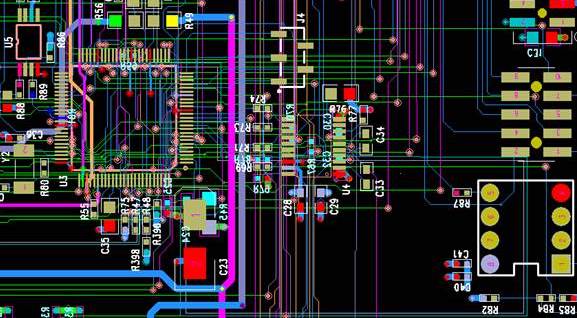
Impedance control is a fundamental requirement in RF PCB design.
Common RF transmission line structures include:
- Microstrip lines
- Stripline structures
- Coplanar waveguides
The characteristic impedance is influenced by:
- Trace width
- Copper thickness
- Dielectric thickness
- Dielectric constant
- Distance to reference planes
For many RF systems, 50Ω impedance is commonly used because it provides a balance between power handling capability and signal transmission efficiency.
Best Practices for Impedance Control
- Define impedance requirements during stack-up design
- Work closely with PCB manufacturers
- Perform impedance simulation before fabrication
- Verify impedance through TDR testing
Proper impedance control helps reduce reflection, signal loss, and RF performance variation.
4. Optimize RF Component Placement
RF PCB layout should begin with a carefully planned component placement strategy.
Minimize RF Signal Path Length
Shorter RF signal paths reduce transmission loss and parasitic effects.
Sensitive RF components such as:
- Antennas
- RF amplifiers
- Filters
- Mixers
- Oscillators
should be positioned to minimize unnecessary routing distance.
Separate Functional Blocks
RF circuits should be divided into functional areas, such as:
- RF signal path
- Analog circuits
- Digital control circuits
- Power supply sections
This prevents digital noise from affecting sensitive RF signals.
5. Pay Attention to RF Routing Design
RF traces require different routing rules compared with standard PCB traces.
Maintain Consistent Trace Geometry
Avoid sudden changes in:
- Trace width
- Reference plane distance
- Routing direction
These changes create impedance discontinuities.
Avoid Sharp Corners
Sharp 90-degree corners can introduce impedance changes and signal reflection.
Better approaches include:
- Using curved traces
- Using 45-degree bends
- Maintaining consistent trace width
Minimize Via Transitions
Every via introduces parasitic effects. Excessive layer transitions may increase insertion loss and reduce signal integrity.
When vias are necessary:
- Use optimized via structures
- Consider via-in-pad technology for compact designs
- Maintain proper grounding around RF transitions
6. Implement Effective Grounding and Shielding
A stable grounding structure is essential for RF performance.
Use Continuous Ground Planes
A continuous reference plane provides a stable return path for RF currents and reduces electromagnetic radiation.
Add Ground Via Stitching
Ground vias around RF transmission lines and sensitive circuits can improve isolation and reduce unwanted coupling.
Consider RF Shielding
Shielding solutions such as metal cans or controlled enclosure structures may be required for high-performance RF systems.
Effective grounding and shielding help control EMI and improve system reliability.
7. Manage Thermal and Power Considerations
Although RF design focuses on signal performance, thermal management is also important.
High-power RF circuits may generate significant heat through:
- Power amplifiers
- Transmit modules
- RF front-end components
Design considerations include:
- Thermal vias
- Copper thickness optimization
- Proper component placement
- Heat dissipation paths
Maintaining stable temperature conditions helps prevent RF performance drift.
8. Consider Manufacturing Requirements During RF PCB Design
A high-performance RF design must also be manufacturable.
Important DFM considerations include:
- Minimum trace width and spacing
- Copper thickness variation
- Layer alignment accuracy
- Surface finish selection
- Material availability
- Controlled impedance capability
Early communication between designers and PCB manufacturers can help identify potential production risks before fabrication.
9. RF PCB Testing and Validation
RF PCB performance should be verified through proper testing methods.
Common RF validation methods include:
Network Analyzer Testing
A Vector Network Analyzer (VNA) can measure:
- Return loss
- Insertion loss
- VSWR
- S-parameters
TDR Testing
Time Domain Reflectometry helps verify impedance consistency along transmission lines.
Environmental Testing
For demanding applications, additional testing may include:
- Temperature cycling
- Humidity testing
- Mechanical reliability testing
Testing ensures the RF PCB meets design requirements under real operating conditions.
10. Applications of RF PCB Technology
RF circuit and PCB design are widely used in:
- 5G communication equipment
- Wireless networking devices
- Radar systems
- Automotive radar sensors
- Satellite communication systems
- IoT devices
- Medical wireless equipment
- Microwave modules
As applications continue moving toward higher frequencies and smaller form factors, RF PCB design requirements will become increasingly demanding.
Conclusion
Designing reliable RF circuits and PCB layouts requires careful consideration of electrical performance, material properties, manufacturing capabilities, and system-level requirements.
Key success factors include:
- Selecting suitable high-frequency PCB materials
- Maintaining controlled impedance
- Optimizing RF routing structures
- Ensuring proper grounding and shielding
- Considering manufacturing limitations early in the design process
By combining RF engineering principles with practical PCB manufacturing knowledge, designers can achieve better signal integrity, lower transmission loss, and improved product reliability in high-frequency electronic applications.

