
As electronic products continue to become faster, smaller, and more integrated, circuit board noise has become a major challenge in PCB design. High-speed processors, switching power supplies, wireless communication modules, and sensitive analog circuits all generate unwanted electrical noise that can affect system performance.
Excessive PCB noise may result in:
- Signal distortion
- Communication errors
- Measurement inaccuracies
- System instability
- Electromagnetic compatibility (EMC) failures
Reducing circuit board noise requires a comprehensive design approach involving schematic planning, PCB layout, power distribution, grounding strategy, and manufacturing control.
This article introduces the major sources of PCB noise and practical methods to improve circuit stability and signal quality.
1. Understanding Circuit Board Noise
Circuit board noise refers to unwanted electrical signals or electromagnetic energy that interfere with normal circuit operation.
Noise can appear in different forms:
- Conducted noise
- Radiated noise
- Power supply noise
- Ground noise
- Crosstalk between signal traces
The impact of noise depends on:
- Signal frequency
- Circuit sensitivity
- PCB structure
- Component arrangement
- System operating environment
2. Common Sources of PCB Noise
2.1 Switching Power Supply Noise
Switching regulators are one of the most common sources of PCB noise.
During switching operation, rapid voltage and current changes generate:
- High-frequency harmonics
- Voltage spikes
- Current ripple
- Electromagnetic radiation
Common noise sources include:
- MOSFET switching nodes
- Inductors
- Diodes
- Transformer windings
Poor PCB layout around switching circuits can significantly increase noise levels.
2.2 High-Speed Digital Signal Noise
Modern processors and communication interfaces operate at high frequencies with fast edge rates.
Examples include:
- DDR memory
- USB interfaces
- Ethernet
- FPGA signals
- High-speed clocks
Rapid signal transitions can generate:
- Reflections
- Crosstalk
- Ground bounce
- EMI radiation
2.3 Grounding Problems
Improper grounding is a major cause of circuit noise.
Common problems include:
- Long ground return paths
- Ground loops
- Shared return paths between noisy and sensitive circuits
These issues increase impedance and allow unwanted noise currents to affect other circuits.
2.4 Electromagnetic Interference (EMI)
Noise generated by PCB traces and components can couple into nearby circuits through electromagnetic fields.
Common coupling paths include:
- Capacitive coupling
- Inductive coupling
- Radiated coupling
Sensitive circuits such as sensors, RF modules, and analog amplifiers are especially vulnerable.
3. Optimize PCB Layout to Reduce Noise
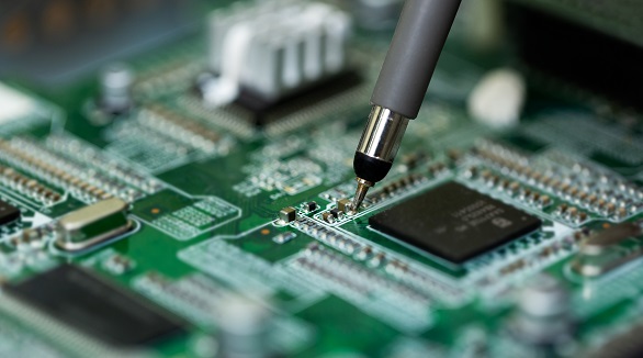
PCB layout has a direct impact on noise performance.
3.1 Separate Functional Circuit Areas
A good PCB layout should divide the board into different functional zones:
- Power supply section
- Digital processing section
- Analog circuit section
- RF communication section
High-noise areas should be separated from sensitive circuits.
For example:
- Keep switching regulators away from analog sensors
- Avoid placing high-speed clocks near RF circuits
- Separate motor drivers from signal processing circuits
3.2 Minimize Current Loop Areas
High-frequency current loops can act as antennas and increase EMI.
To reduce radiation:
- Keep power switching loops compact
- Place related components close together
- Minimize unnecessary trace length
This is especially important for:
- DC-DC converters
- Motor control circuits
- High-current drivers
3.3 Use Proper PCB Stack-Up Design
A well-designed multilayer PCB stack-up improves noise control.
Recommended practices:
- Use continuous ground planes
- Place high-speed signals close to reference planes
- Avoid unnecessary plane splits
- Maintain controlled impedance structures
Ground planes provide low-impedance return paths and reduce electromagnetic radiation.
4. Improve Grounding Design
Grounding is one of the most effective methods for reducing PCB noise.
4.1 Use Solid Ground Planes
A continuous ground plane helps:
- Reduce return path impedance
- Improve signal integrity
- Minimize EMI
Avoid routing high-speed signals across gaps or breaks in ground planes.
4.2 Optimize Ground Return Paths
High-frequency currents follow the path of least impedance.
Good practices include:
- Keep return paths short
- Provide nearby ground vias
- Avoid shared noisy return paths
4.3 Separate Analog and Digital Grounds Correctly
Analog and digital circuits often have different noise sensitivities.
However, completely separating grounds without proper design may create unexpected current paths.
A better approach is to:
- Understand current flow
- Control return paths
- Connect grounds at appropriate locations
5. Improve Power Integrity
Stable power delivery is essential for reducing noise.
5.1 Add Proper Decoupling Capacitors
Decoupling capacitors help suppress high-frequency power noise.
Recommended placement:
- Close to IC power pins
- Short connection to ground
- Suitable capacitor values for different frequencies
5.2 Optimize Power Distribution Network (PDN)
A good PDN reduces:
- Voltage fluctuations
- Power ripple
- Transient noise
Important factors include:
- Power plane design
- Capacitor arrangement
- Trace impedance
- Current capacity
5.3 Filter Power Supply Noise
Filtering methods include:
- LC filters
- Ferrite beads
- Common-mode chokes
- EMI filters
These components help prevent noise from spreading between circuit sections.
6. Control Signal Integrity Issues
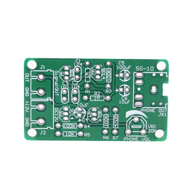
Signal integrity problems can create noise and system errors.
6.1 Control Impedance
For high-speed signals, PCB traces should maintain controlled impedance.
Factors affecting impedance include:
- Trace width
- Dielectric thickness
- Copper thickness
- PCB material
Proper impedance control reduces:
- Signal reflections
- Ringing
- Overshoot
6.2 Reduce Crosstalk
Crosstalk occurs when signals interfere with nearby traces.
Methods to reduce crosstalk:
- Increase spacing between traces
- Avoid long parallel routing
- Use ground shielding traces
- Maintain proper reference planes
6.3 Match Differential Signals
Differential pairs should maintain:
- Equal trace length
- Consistent spacing
- Symmetrical routing
This improves noise immunity for interfaces such as:
- USB
- Ethernet
- LVDS
- PCIe
7. Use Shielding and Filtering Techniques
For applications with strict EMC requirements, additional protection may be needed.
7.1 PCB Shielding
Shielding methods include:
- Metal shielding covers
- Conductive coatings
- Grounded shielding structures
These reduce electromagnetic coupling between circuit sections.
7.2 EMI Filters
Filters can suppress unwanted frequencies.
Common solutions include:
- Capacitor filters
- LC networks
- Ferrite components
The correct filter design depends on the noise frequency range.
8. Thermal Management and Noise Reduction
Temperature changes can also influence circuit noise.
High temperatures may cause:
- Increased component resistance
- Parameter variation
- Reduced signal stability
Thermal management methods include:
- Larger copper areas
- Thermal vias
- Proper component spacing
- Heat dissipation structures
Stable temperature conditions improve long-term electrical performance.
9. PCB Manufacturing Factors Affecting Noise
PCB fabrication quality also influences noise performance.
Important factors include:
Material Selection
High-speed and RF applications may require low-loss materials with stable dielectric properties.
Impedance Control
Manufacturing variation in:
- Trace width
- Dielectric thickness
- Copper thickness
can affect signal performance.
Layer Alignment Accuracy
Poor registration may affect:
- Differential impedance
- Signal return paths
- High-speed performance
Therefore, close cooperation between PCB designers and manufacturers is important.
10. Testing and Verification Methods
Noise problems should be evaluated through testing.
Common methods include:
Oscilloscope Measurement
Used to analyze:
- Voltage ripple
- Signal ringing
- Switching noise
Spectrum Analyzer Testing
Used to identify:
- EMI sources
- Frequency components
- Radiation problems
EMC Compliance Testing
Includes:
- Conducted emission testing
- Radiated emission testing
- Immunity testing
Early testing helps identify problems before mass production.
Common Mistakes That Increase PCB Noise
Typical design issues include:
- Long high-current loops
- Poor grounding strategy
- Incorrect capacitor placement
- Routing sensitive signals near switching circuits
- Ignoring impedance control
- Insufficient EMI protection
Avoiding these problems during the design stage can significantly improve product reliability.
Conclusion
Reducing circuit board noise requires a combination of proper PCB layout, grounding optimization, power integrity management, signal integrity control, and EMC design practices.
The key methods include:
- Optimizing PCB layout and current paths
- Designing effective grounding structures
- Improving power distribution networks
- Controlling high-speed signal behavior
- Applying shielding and filtering techniques
By considering noise control from the early design stage, engineers can improve signal quality, reduce electromagnetic interference, and create more reliable electronic products.
