
The solder mask is one of the most important layers in printed circuit board (PCB) manufacturing. Although it appears as a simple colored coating on the PCB surface, it plays a critical role in protecting circuits, improving assembly reliability, and ensuring long-term electrical performance.
In modern electronic products, PCBs are becoming increasingly compact with:
- Smaller component packages
- Higher routing density
- Finer trace spacing
- More complex assembly processes
As a result, the requirements for solder mask technology continue to increase.
A properly designed and manufactured solder mask helps prevent:
- Solder bridges
- Copper oxidation
- Electrical short circuits
- Environmental damage
- Assembly defects
This article explains what PCB solder mask is, how it works, the manufacturing process, design considerations, and its impact on PCB reliability.
1. What Is PCB Solder Mask?
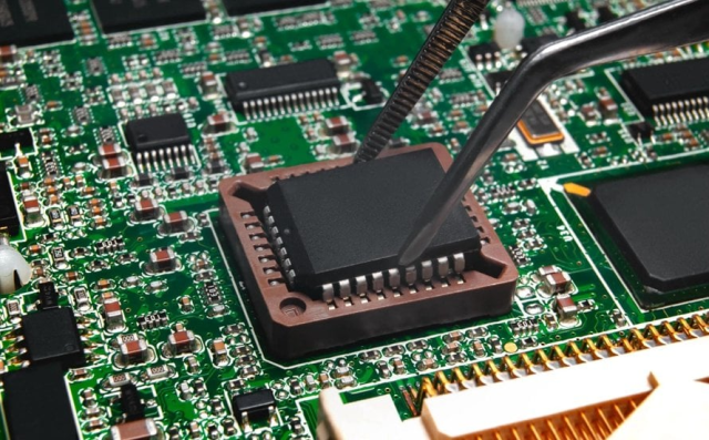
PCB solder mask, also known as solder resist, is a protective insulating layer applied over the copper traces of a printed circuit board.
Its main functions are:
- Protect exposed copper from oxidation
- Prevent unwanted solder connections
- Provide electrical insulation
- Improve PCB durability
The solder mask is usually applied to both sides of a PCB:
- Top solder mask
- Bottom solder mask
The most common solder mask color is green, but other colors are also available, including:
- Blue
- Black
- Red
- White
- Yellow
The color does not determine electrical performance; it mainly serves identification and manufacturing purposes.
2. How Does PCB Solder Mask Work?
The solder mask works by selectively covering areas of copper while leaving specific locations exposed for soldering.
The basic principle is:
Protect the circuit → expose connection points → control solder flow
2.1 Protecting Copper Traces
Copper is highly conductive but can oxidize when exposed to air and moisture.
Oxidized copper may cause:
- Poor solderability
- Increased resistance
- Reduced connection reliability
The solder mask acts as a barrier between copper and the external environment.
2.2 Preventing Solder Bridges
During SMT assembly, solder paste is applied to component pads and melted during reflow soldering.
Without solder mask protection, molten solder may spread between nearby traces.
This can create:
- Short circuits
- Assembly failures
- Electrical defects
The solder mask defines the soldering area and helps maintain separation between conductive regions.
2.3 Improving Electrical Insulation
The solder mask provides insulation between adjacent copper features.
This is especially important for:
- High-density PCB designs
- Fine-pitch components
- High-voltage circuits
Proper solder mask thickness helps improve:
- Insulation reliability
- Voltage resistance
- Long-term stability
3. PCB Solder Mask Manufacturing Process
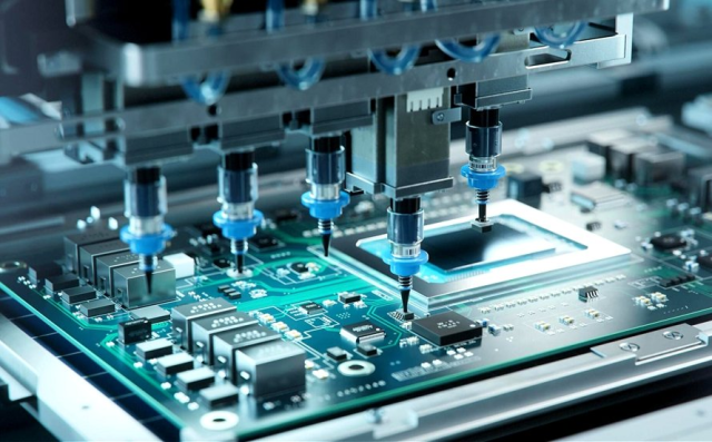
The solder mask application process involves several precision-controlled steps.
3.1 PCB Surface Preparation
Before applying solder mask, the PCB surface is cleaned.
The purpose is to remove:
- Dust
- Oxides
- Contaminants
- Processing residues
A clean copper surface ensures strong solder mask adhesion.
3.2 Solder Mask Coating
The solder mask material is applied to the PCB surface.
Common application methods include:
- Screen printing
- Curtain coating
- Spray coating
The coating must achieve:
- Uniform thickness
- Good coverage
- Strong adhesion
3.3 Pre-Curing
After coating, the PCB undergoes initial curing.
This stabilizes the solder mask layer before imaging.
3.4 Exposure and Imaging
A photolithography process is used to define areas where solder mask should remain or be removed.
UV exposure transfers the solder mask pattern onto the PCB.
The exposed areas correspond to:
- Component pads
- Test points
- Connector contacts
3.5 Development
The unwanted solder mask material is removed.
The remaining solder mask protects the required copper areas while exposing soldering locations.
3.6 Final Curing
The PCB undergoes final curing at controlled temperatures.
This improves:
- Mechanical strength
- Chemical resistance
- Thermal stability
4. Types of PCB Solder Mask Materials
Different applications may require different solder mask technologies.
4.1 Liquid Photoimageable (LPI) Solder Mask
LPI is the most common solder mask type.
Advantages:
- High precision
- Suitable for fine-pitch PCB designs
- Good process compatibility
Applications:
- SMT PCBs
- HDI PCBs
- Multilayer PCBs
4.2 Dry Film Solder Mask
Dry film solder masks provide higher thickness control.
Advantages:
- Good uniformity
- Suitable for specific high-density applications
4.3 Thermal Cure Solder Mask
Thermal curing provides:
- Strong adhesion
- Good durability
Often used for:
- Industrial applications
- High-reliability electronics
5. Important PCB Solder Mask Parameters
5.1 Solder Mask Thickness
Typical solder mask thickness depends on:
- PCB design
- Manufacturing requirements
- Application environment
Too thin:
- Reduced protection
- Lower insulation capability
Too thick:
- May affect soldering accuracy
- May interfere with fine-pitch components
5.2 Solder Mask Opening
The opening defines the exposed copper area.
Incorrect opening design may cause:
- Poor solder joints
- Solder bridging
- Component placement issues
5.3 Solder Mask Registration
Registration refers to the alignment accuracy between:
- Solder mask layer
- Copper pattern
Poor registration may result in:
- Covered pads
- Exposed unwanted copper
- Assembly defects
6. Solder Mask Requirements for SMT Assembly
Modern SMT assembly requires precise solder mask control.
Important considerations include:
6.1 Fine-Pitch Components
Components such as:
- BGA
- QFN
- CSP
require accurate solder mask definition.
Challenges include:
- Small pad spacing
- Tight manufacturing tolerance
6.2 Solder Mask Defined (SMD) vs Non-Solder Mask Defined (NSMD)
Solder Mask Defined (SMD)
The solder mask overlaps the pad edge.
Advantages:
- Stronger mechanical support
Applications:
- Some BGA designs
Non-Solder Mask Defined (NSMD)
The copper pad is larger than the solder mask opening.
Advantages:
- Better solder joint formation
- Common in fine-pitch SMT
Applications:
- Advanced SMT assembly
7. Solder Mask Considerations for High-Performance PCBs
7.1 High-Frequency PCB Applications
For RF and microwave PCBs, solder mask selection may affect:
- Dielectric characteristics
- Signal loss
- Impedance performance
Engineers must consider:
- Solder mask dielectric properties
- Coverage requirements
- High-frequency signal areas
7.2 High-Voltage PCB Applications
For power electronics, solder mask contributes to:
- Insulation protection
- Creepage distance management
Applications include:
- EV power systems
- Industrial power supplies
- High-voltage converters
7.3 Flexible PCB Applications
For FPCs, solder mask must maintain:
- Flexibility
- Adhesion
- Mechanical durability
8. Common Solder Mask Defects
8.1 Solder Mask Misalignment
Causes:
- Poor registration control
- Manufacturing variation
Effects:
- Pad coverage
- Reduced soldering reliability
8.2 Solder Mask Peeling
Possible causes:
- Poor surface preparation
- Incorrect curing process
Effects:
- Copper exposure
- Reduced protection
8.3 Uneven Solder Mask Thickness
Effects:
- Assembly problems
- Insulation inconsistency
8.4 Pinholes and Voids
Small defects may expose copper and reduce protection.
9. How Solder Mask Affects PCB Reliability
A high-quality solder mask improves:
Electrical Reliability
By preventing:
- Short circuits
- Leakage paths
- Copper oxidation
Mechanical Reliability
By protecting:
- Copper traces
- Solder joints
Manufacturing Reliability
By improving:
- Solder process control
- Assembly yield
- Inspection accuracy
Conclusion
PCB solder mask is a critical protective layer that directly affects PCB manufacturing quality and product reliability.
Although it may appear to be only a surface coating, solder mask technology plays an essential role in:
- Protecting copper circuits
- Preventing solder defects
- Improving electrical insulation
- Supporting advanced SMT assembly
As electronic products continue moving toward higher density, smaller size, and higher performance, precise solder mask design and manufacturing control will remain essential for reliable PCB production.
