
The SPI (Serial Peripheral Interface) is a widely used synchronous communication protocol in embedded systems, commonly applied for communication between:
- Microcontrollers (MCUs)
- Sensors
- Memory devices
- ADC/DAC converters
- Display controllers
- Communication modules
Unlike protocols such as I²C, which use open-drain signaling and require pull-up resistors by design, SPI typically uses push-pull drivers. This leads to a common design question:
Can pull-up resistors be used on SPI lines?
The short answer is:
Yes, pull-up resistors can be used on SPI lines, but they are not normally required and should only be added for specific design purposes.
Understanding when and why to use them is important for ensuring reliable SPI communication.
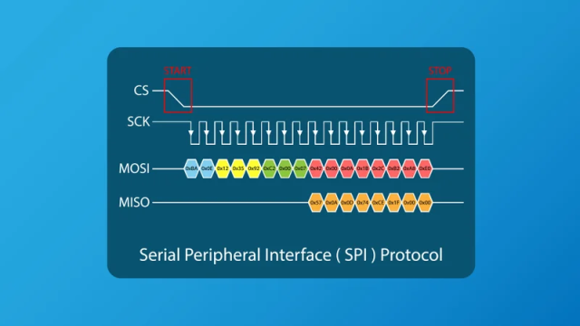
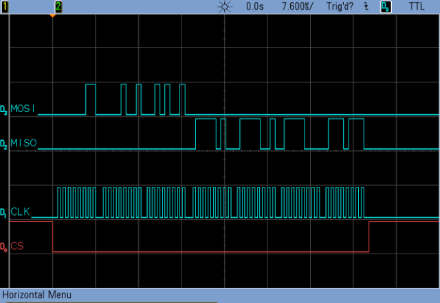
1. Basic Structure of SPI Communication
A typical SPI interface consists of four signal lines:
| Signal | Function |
|---|---|
| SCLK | Serial Clock |
| MOSI | Master Output Slave Input |
| MISO | Master Input Slave Output |
| CS/SS | Chip Select |
SPI communication usually follows a master-slave architecture:
- The master generates the clock signal.
- The master controls chip selection.
- Data is transferred through MOSI and MISO.
Unlike I²C, SPI devices actively drive signals both HIGH and LOW through push-pull output stages.
2. Why SPI Usually Does Not Require Pull-up Resistors
2.1 Push-Pull Output Structure
SPI devices normally use push-pull outputs.
A push-pull driver contains:
- A transistor pulling the signal HIGH
- A transistor pulling the signal LOW
This allows the device to actively control the logic state.
For example:
When SCLK needs to be HIGH:
- The output transistor drives the line upward.
When SCLK needs to be LOW:
- Another transistor pulls the line downward.
Therefore, unlike open-drain systems, SPI does not rely on external resistors to define logic levels.
2.2 SPI Signal Speed Requirements
SPI communication often operates at relatively high speeds:
- Several MHz
- Tens of MHz
- Sometimes hundreds of MHz
A pull-up resistor combined with PCB trace capacitance creates an RC charging effect.
The rise time can be approximated as:
t = 2.2 × R × C
Where:
- t = signal rise time
- R = pull-up resistance
- C = total line capacitance
A large resistor value may cause:
- Slow rising edges
- Signal distortion
- Timing errors
This is why SPI generally avoids relying on pull-up resistors for signal transitions.
3. When Can Pull-up Resistors Be Used on SPI Lines?
Although unnecessary in most cases, pull-up resistors can be useful in certain situations.
3.1 Pull-up Resistor on Chip Select (CS/SS)
This is the most common application.
Purpose:
Prevent accidental device selection during:
- MCU reset
- Power-up sequence
- High-impedance states
Example:
VCC
 |
10kΩ
 |
CS Line
 |
SPI Slave
When the MCU is not driving the CS signal:
- The pull-up keeps CS HIGH.
- The slave remains inactive.
This helps avoid:
- False communication
- Unwanted data transmission
- Device initialization problems
Typical values:
- 4.7 kΩ
- 10 kΩ
- 47 kΩ
3.2 Pull-up Resistor on MISO Line
A pull-up resistor may be used when multiple SPI slaves share the same MISO line.
Problem:
When a slave is not selected:
- Its MISO output should enter a high-impedance state.
If this behavior is unreliable, the line may become:
- Floating
- Noise sensitive
A weak pull-up can provide a defined idle state.
However, the designer must confirm:
- The slave supports tri-state output.
- Multiple devices will not drive the line simultaneously.
3.3 Pull-up Resistor for Level Translation
Sometimes SPI connects devices operating at different voltage levels.
Example:
- MCU: 1.8 V
- Peripheral: 3.3 V
A pull-up resistor may be part of a level-shifting solution.
However, simple resistor-based level shifting is usually unsuitable for high-speed SPI because it may introduce:
- Slow edges
- Signal distortion
Dedicated level translators are usually preferred.
3.4 Pull-up Resistor for Open-Drain SPI Implementations
Some special devices implement SPI-like communication using open-drain outputs.
In such cases, pull-ups may be required.
Examples:
- Custom communication interfaces
- Special sensor modules
- Mixed-protocol designs
The resistor functions similarly to I²C pull-ups.
4. Risks of Incorrect Pull-up Resistor Usage
4.1 Excessive Signal Loading
A low-value pull-up resistor creates additional current consumption.
Example:
With:
- 3.3 V supply
- 1 kΩ resistor
Current:
I = V/R
I = 3.3 mA
Multiple pull-ups may increase power consumption.
4.2 Reduced Signal Speed
A large RC time constant can cause:
- Slow rising edges
- Reduced noise margin
- Timing violations
This is especially important for:
- High-frequency SPI
- Long PCB traces
- Flexible cables
4.3 Driver Conflict
Adding pull-ups does not solve situations where two devices drive the same SPI line.
For example:
- One device outputs HIGH.
- Another device outputs LOW.
This creates:
- Excessive current
- Possible device damage
Proper chip select control is required.
5. Recommended Pull-up Resistor Values for SPI
There is no universal value because it depends on:
- SPI frequency
- Trace length
- Voltage level
- Device characteristics
Common design choices:
| Application | Typical Value |
|---|---|
| CS pull-up | 4.7 kΩ – 10 kΩ |
| MISO idle control | 10 kΩ – 47 kΩ |
| Low-speed SPI | 10 kΩ |
| High-speed SPI | Usually avoid pull-ups |
The final value should be verified through:
- Datasheet requirements
- Signal integrity simulation
- Oscilloscope measurements
6. SPI PCB Layout Considerations
Pull-up resistors alone cannot guarantee reliable SPI communication.
PCB design should also consider:
6.1 Keep SPI Traces Short
Long traces increase:
- Capacitance
- Reflection
- EMI radiation
6.2 Maintain Proper Ground Reference
SPI signals should have:
- Continuous ground plane
- Controlled return path
This reduces:
- Crosstalk
- Noise coupling
6.3 Add Series Resistors When Needed
For high-speed SPI, series termination resistors are often more effective than pull-ups.
Typical values:
- 22 Ω
- 33 Ω
- 47 Ω
They help reduce:
- Ringing
- Overshoot
- Signal reflection
6.4 Consider Clock Signal Priority
The SPI clock line is usually the most sensitive signal.
Layout recommendations:
- Keep SCLK short.
- Avoid routing near noisy power circuits.
- Maintain spacing from high-current traces.
7. Comparison: Pull-up Requirements Between SPI and I²C
| Feature | SPI | I²C |
|---|---|---|
| Output type | Push-pull | Open-drain |
| Pull-up required | Usually no | Yes |
| Main purpose | Optional idle control | Logic level generation |
| Speed limitation | Less affected | Strongly affected by RC |
| Typical use | CS/MISO control | SDA/SCL |
8. Practical Design Recommendations
For most SPI PCB designs:
- Add pull-up resistors on CS lines if devices require a defined inactive state.
- Consider pull-ups on MISO when multiple slaves share the bus.
- Avoid using pull-ups as a replacement for proper signal integrity design.
- For high-speed SPI, prioritize:
- Trace impedance control
- Series termination
- Ground reference
- Signal timing analysis
Conclusion
Pull-up resistors can be used on SPI lines, but unlike I²C, they are not a fundamental requirement of the protocol.
In most SPI applications:
- CS pull-ups are commonly recommended to prevent unintended device activation.
- MISO pull-ups may help in multi-device configurations.
- SCLK and MOSI pull-ups are usually unnecessary because SPI uses push-pull drivers.
Reliable SPI communication depends mainly on proper PCB design, including:
- Short signal paths
- Good grounding
- Controlled impedance
- Appropriate termination methods
For industrial and high-speed electronic systems, early consideration of SPI signal integrity during PCB design can significantly improve communication stability and product reliability.
