
In premium audio systems, the PCB is not simply a platform for connecting electronic components. It plays a critical role in maintaining signal purity, low noise performance, power stability, and long-term reliability.
High-fidelity (Hi-Fi) audio amplifier designs require the PCB to handle both low-level analog audio signals and high-current power amplification circuits within the same system. Poor PCB design or manufacturing decisions may introduce issues such as:
- Background noise
- Signal distortion
- Ground interference
- Channel imbalance
- Thermal instability
During the transition from prototype validation to production, engineers must consider not only circuit performance but also PCB-level factors including:
- Analog signal routing
- Grounding strategy
- Power distribution
- Thermal management
- Component placement
- Manufacturing consistency
This case study presents how KKPCB supported a high-fidelity audio amplifier PCB project by optimizing PCB design and manufacturing considerations to improve product reliability and production readiness.
1. Project Background
The project involved the development of a high-performance audio amplifier PCB designed for premium audio applications.
The customer required a PCB solution capable of supporting:
- High-quality analog audio transmission
- Stable power amplification
- Low-noise operation
- Reliable long-term performance
The main challenge was maintaining audio signal integrity while managing the high-current power section within a limited PCB space.
2. Key PCB Design Challenges
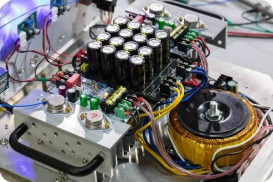
2.1 Low-Level Audio Signal Integrity Control
Audio amplifier circuits contain sensitive analog signal paths where even small amounts of interference may affect sound quality.
Potential PCB-level risks included:
- Noise coupling from power circuits
- Ground loop interference
- Signal path interference
- Unnecessary trace coupling
For high-fidelity audio applications, PCB layout must minimize unwanted electrical noise while maintaining a clean signal path.
2.2 Power Distribution and Current Handling
The amplifier power stage requires stable current delivery.
PCB design challenges included:
- High-current trace capability
- Power plane optimization
- Voltage drop reduction
- Heat generation control
Insufficient power routing could lead to:
- Output instability
- Reduced amplifier efficiency
- Thermal stress
2.3 Grounding and Noise Reduction
Grounding is one of the most important aspects of audio PCB design.
Improper grounding may introduce:
- Hum noise
- Signal interference
- Channel crosstalk
The PCB required careful consideration of:
- Analog ground
- Power ground
- Signal return paths
- Ground separation strategy
2.4 Thermal Management
During operation, power amplifier circuits generate significant heat.
Thermal challenges included:
- Heat concentration around power components
- Copper distribution optimization
- Component temperature control
Poor thermal management may affect:
- Component lifetime
- Output stability
- Product reliability
3. KKPCB Engineering Support and Solutions
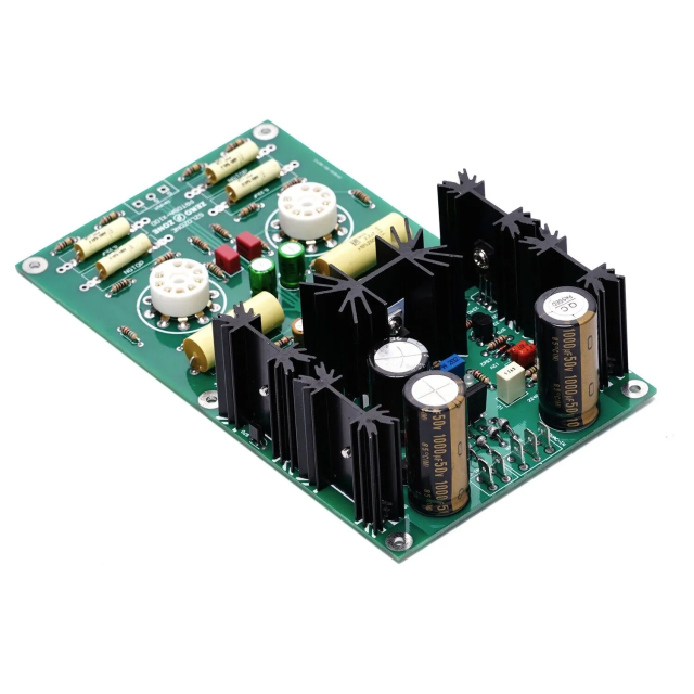
3.1 PCB Layout Optimization
KKPCB engineering team reviewed the PCB layout with focus on:
- Signal path optimization
- Component placement
- Power routing
- Grounding structure
The layout was adjusted to reduce interference between:
- Sensitive analog circuits
- High-current power sections
3.2 Improved Grounding Strategy
To enhance audio signal stability, the PCB structure was optimized by:
- Improving ground return paths
- Reducing unnecessary ground loops
- Separating sensitive signal areas from noisy circuits
This helped improve:
- Noise control
- Signal consistency
- Audio performance reliability
3.3 Power and Thermal Design Optimization
For the amplifier power stage, KKPCB provided recommendations including:
- Optimized copper area distribution
- Enhanced current-carrying capability
- Improved thermal paths
These improvements helped ensure stable operation under continuous load conditions.
3.4 Manufacturing Feasibility Review (DFM)
Before production, KKPCB conducted a DFM review covering:
- PCB manufacturability
- Component placement feasibility
- Soldering requirements
- Assembly reliability
Potential production risks were identified early to improve:
- Manufacturing efficiency
- First-pass yield
- Production consistency
4. Manufacturing Considerations
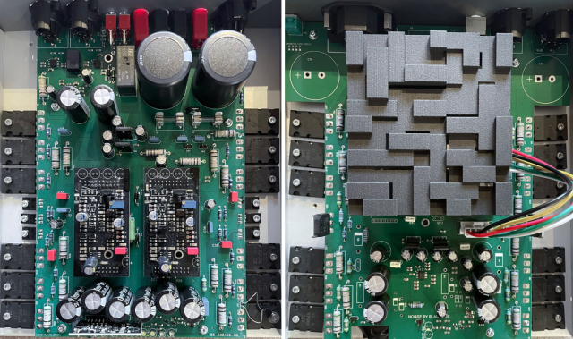
4.1 PCB Material Selection
The PCB material was evaluated according to:
- Electrical requirements
- Thermal requirements
- Mechanical reliability
Suitable material selection helps maintain stable performance throughout product operation.
4.2 Copper Thickness and Current Capacity
For power amplifier applications, copper thickness is an important factor affecting:
- Current carrying capability
- Heat dissipation
- Long-term reliability
The PCB structure was reviewed to ensure sufficient copper capacity for power sections.
4.3 Surface Finish Selection
A suitable surface finish helps ensure:
- Reliable solder joints
- Long-term corrosion resistance
- Assembly consistency
Common options include:
- ENIG
- ENEPIG
depending on application requirements.
5. Project Results
Through PCB design optimization and manufacturing support, KKPCB helped improve the overall production readiness of the audio amplifier PCB.
Key improvements included:
- Improved analog signal routing stability
- Reduced interference risks between power and signal sections
- Enhanced thermal reliability
- Improved manufacturing consistency
The optimized PCB structure provided a stronger foundation for:
- High-quality audio performance
- Stable mass production
- Long-term product reliability
6. Key Engineering Insights
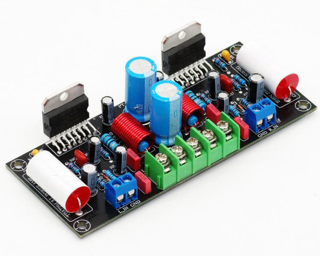
For high-fidelity audio amplifier PCB development, several PCB-level factors should be considered early:
Signal Integrity
Sensitive audio signals require:
- Short signal paths
- Proper routing
- Noise isolation
Grounding Design
A suitable grounding strategy helps reduce:
- Noise
- Crosstalk
- Signal distortion
Power Integrity
Stable power delivery requires:
- Proper copper design
- Optimized power paths
- Thermal consideration
Manufacturing Readiness
Early DFM review helps prevent:
- Production defects
- Assembly issues
- Reliability risks
Conclusion
A high-fidelity audio amplifier PCB requires more than basic circuit connectivity. The PCB design and manufacturing process directly influence:
- Audio signal quality
- Noise performance
- Power stability
- Product reliability
Through engineering collaboration, PCB layout optimization, DFM analysis, and manufacturing process control, KKPCB supported the transition of a premium audio amplifier PCB from design validation toward reliable production.
For complex electronic products requiring precise signal performance and manufacturing consistency, early PCB engineering involvement can help identify potential risks and improve overall product success.
