
The CLTE™ Series laminates are engineered for high-frequency RF, microwave, and millimeter-wave PCB applications where signal integrity, dimensional stability, and manufacturing consistency are essential. With low dielectric loss, excellent thermal reliability, and outstanding mechanical performance, these PTFE-based laminates are widely used in radar systems, satellite communications, aerospace electronics, 5G infrastructure, and high-speed networking equipment.
At KKPCB, we specialize in fabricating high-frequency PCBs using advanced RF laminates. Through optimized manufacturing processes and strict process control, we ensure consistent electrical performance from prototype development to volume production.
1. Material Storage and Handling
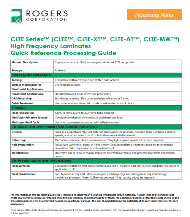
Proper storage is the first step toward maintaining laminate performance throughout fabrication.
Recommended Storage Conditions
- Store laminates horizontally on a flat surface.
- Keep materials in a clean, dry, temperature-controlled environment.
- Recommended storage temperature: 20–25°C
- Recommended relative humidity: below 50% RH
Handling Best Practices
- Wear lint-free gloves to avoid contamination from fingerprints or oils.
- Prevent scratches, bending, or excessive mechanical stress.
- Handle PTFE laminates carefully to avoid edge damage before processing.
Proper material handling helps preserve dielectric consistency and dimensional accuracy during fabrication.
2. Precision Drilling
Accurate drilling is critical for maintaining reliable via structures and multilayer alignment.
Recommended Tooling
- Carbide drill bits
- Diamond-coated drill bits for extended tool life
Typical Drilling Parameters
| Parameter | Recommended Value |
|---|---|
| Entry Speed | 150–180 SFM |
| Retract Speed | 350–400 SFM |
Process Recommendations
- Match entry and backup materials to laminate hardness.
- Optimize drilling parameters to minimize resin smear and burr formation.
- Perform controlled deburring after drilling to prevent dielectric damage.
3. Copper Etching
CLTE laminates are compatible with conventional PCB etching processes when properly optimized.
Recommended practices include:
- Maintain stable etching rates.
- Minimize conductor undercut.
- Ensure accurate trace width control.
- Verify fine-line dimensions for impedance-critical RF circuits.
Consistent etching improves impedance accuracy and minimizes insertion loss.
4. Lamination Process
Proper lamination ensures excellent layer bonding and long-term mechanical stability.
Pre-Bake
Remove residual moisture before lamination.
- Temperature: 150°C
- Duration: 30–60 minutes
Lamination Parameters
| Parameter | Recommended Range |
|---|---|
| Temperature | 200–220°C |
| Pressure | 200–300 psi |
| Hold Time | 30–60 minutes |
Cooling
Maintain pressure throughout the controlled cooling cycle to reduce:
- Resin voids
- Layer separation
- PCB warpage
A well-controlled lamination process improves dimensional stability and multilayer reliability.
5. Copper Plating
Uniform copper deposition is essential for RF performance and via reliability.
Surface Preparation
Before plating:
- Remove oxidation and contaminants.
- Perform plasma or chemical surface activation.
- Ensure complete surface cleanliness.
Recommended Plating Processes
Both methods are suitable:
- Electroless copper plating
- Electrolytic copper plating
Maintain consistent copper thickness across the PCB to support stable impedance and signal transmission.
6. PCB Routing and Profiling
Precision profiling minimizes edge defects and preserves laminate integrity.
Recommended Equipment
- CNC routing with carbide tools
- Diamond-coated routing tools
- Laser cutting for high-precision RF structures
Process Optimization
Optimize spindle speed and feed rate to reduce:
- Edge chipping
- Delamination
- Surface roughness
Clean profile edges contribute to improved mechanical reliability and assembly quality.
7. Process Control Recommendations
For high-frequency PCB fabrication, consistent process control is just as important as material selection.
KKPCB recommends:
- Maintaining clean manufacturing environments throughout production.
- Monitoring critical fabrication parameters in real time.
- Verifying impedance and dimensional accuracy during each production stage.
- Performing comprehensive electrical inspection before shipment.
These practices help ensure excellent RF performance, high manufacturing yield, and long-term product reliability.
Quick Reference Guide
| Process | Key Parameter | Recommended Value |
|---|---|---|
| Storage Temperature | Environment | 20–25°C |
| Storage Humidity | RH | <50% |
| Pre-Bake | Temperature | 150°C |
| Pre-Bake Time | Duration | 30–60 min |
| Lamination Temperature | Process | 200–220°C |
| Lamination Pressure | Process | 200–300 psi |
| Lamination Hold Time | Process | 30–60 min |
| Drill Entry Speed | Tooling | 150–180 SFM |
| Drill Retract Speed | Tooling | 350–400 SFM |
Conclusion
The CLTE™ Series provides an excellent material platform for high-frequency RF and microwave PCBs, but achieving optimal electrical performance depends on precise fabrication techniques. From controlled storage and precision drilling to optimized lamination, plating, and routing, every manufacturing step influences signal integrity and long-term reliability.
With extensive experience in PTFE, Rogers®, and other high-frequency laminate processing, KKPCB combines advanced manufacturing capabilities with rigorous quality control to deliver reliable RF PCB solutions for applications ranging from 5G communications and satellite systems to radar, aerospace, and high-speed networking.

