
An Aerospace PCB for a navigation receiver must prevent small phase changes from becoming timing, bearing, or coherent-combining errors long before the board shows an obvious electrical failure. Engineers searching for an Aerospace PCB phase-stability solution should begin by separating clock behavior, RF path mismatch, thermal gradients, and calibration repeatability. The board cannot correct an unstable reference or an undefined system requirement, but its geometry and thermal interfaces can prevent avoidable drift from being added.
This design review uses the AD9361 as a public example of an integrated dual-channel transceiver and clocking architecture, not as a space-qualified part recommendation. Analog Devices describes the device for cellular and general-purpose radio systems; an aerospace program must independently establish part suitability, radiation assurance, screening, and qualification. The useful question here is narrower: how should the receiver PCB preserve predictable phase behavior across its intended operating and test conditions?
Aerospace PCB phase stability starts with an error budget
Phase error can originate in the reference source, PLL behavior, RF filters, connectors, transmission lines, vias, and temperature-dependent electrical delay. A useful first pass converts timing mismatch into phase using Δφ = 360° × f × Δt. As a simple calculation, 1 ps of differential delay corresponds to 0.36° at 1 GHz and 1.8° at 5 GHz.
Those values are arithmetic illustrations, not an acceptance limit; the system owner must set the allowable phase error from the navigation, array, ranging, or coherent-processing budget. For an Aerospace PCB, this conversion turns a system allocation into a discussion about total path delay, not a universal trace-length tolerance. The Aerospace PCB specification should separate that system budget from the fabrication tolerance used to control the finished geometry.
Split the budget into repeatable static offset, unit-to-unit variation, temperature-related drift, power-cycle behavior, and calibration residual. A system architecture review for an Aerospace PCB should state which portion may be corrected in software and which must be controlled by the RF hardware. This prevents a layout team from trying to solve all phase movement with equal-length traces. For example, a matched line pair cannot compensate for a reference clock that restarts with an uncontrolled phase relationship, nor can a calibration table correct an undocumented connector substitution.
An early signal-integrity layout review should therefore put the phase budget beside the interface and calibration requirements.
Keep receiver RF paths electrically comparable
For dual-channel or multi-antenna receivers, preserve comparable stackup, copper environment, launch geometry, and return-plane continuity from each input connector through the filtering and gain stages. Matching only the drawn centerline length misses differences in via count, pad capacitance, bends, reference-plane changes, solder-mask openings, and connector launch details. These discontinuities can alter both loss and group delay, even where the schematic shows nominally identical channels. On an Aerospace PCB, compare the finished channel geometry with the model assumptions at the same connector and measurement planes.
Use the same layer and reference structure where practical. If routing forces one channel to change layers, model the transition with its actual anti-pad, nearby ground returns, connector footprint, and local plane geometry. Keep sensitive inputs away from fast digital edges and switching regulators; where separation is impossible, define the shared return path and shielding boundary instead of relying on a vague keep-out. Review the assembled launch as part of the Aerospace PCB channel, because the board-edge connector and enclosure can change the electromagnetic boundary conditions.
Before routing is frozen, ask the RF designer to identify which path properties matter: insertion loss, phase match, amplitude balance, isolation, or a combination. A controlled-impedance RF build needs the approved dielectric construction, copper thickness, and finished geometry to be part of the model. Do not assign a universal trace-width or phase-match tolerance: calculate from the selected laminate, frequency, stackup, manufacturing variation, and the system-level limit. The Aerospace PCB drawing should identify which RF dimensions are controlled features and which are nominal routing geometry.
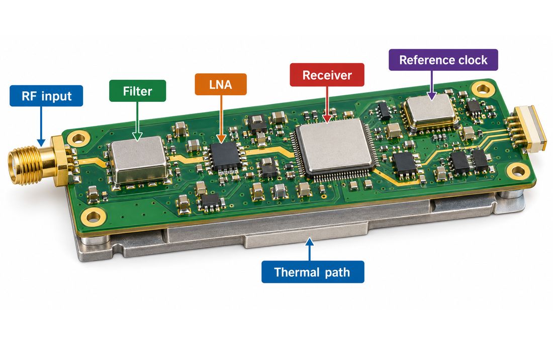
Thermal symmetry is a phase-design variable
Receiver channels can see different temperatures when one sits beside a power amplifier, DC/DC converter, FPGA, or warm mechanical wall. That imbalance can change component phase response, oscillator frequency, filter characteristics, and the physical dimensions of the signal path. In a compact avionics enclosure, the hottest device may not be on the receiver board at all: heat can arrive through a shared baseplate, fastener, shield can, or adjacent assembly.
Map heat sources and heat-spreading paths before component placement is final. Avoid placing one channel next to a heat source while the other sits near an edge or ventilation boundary. If a metal spreader is used, verify that its contact pressure, interface material, and attachment points do not create an asymmetric mechanical or thermal condition. A thermal path is a design feature that needs a drawing and tolerance, not just a colored simulation image.
For this Aerospace PCB, also document the carrier contact surface and any interface material that affects heat flow. Incorporate this review into Aerospace PCB fabrication planning so copper balance, plane structure, mounting lands, and board thickness match the thermal assumptions.
Thermocouples or temperature sensors placed only at the enclosure inlet can miss local gradients across the RF section. A thermal-gradient management plan should assign sensor locations to the actual sensitive components and interfaces. Define measurement locations near the reference source, channel filters, active gain devices, and board-to-carrier contact.
The test plan should record the thermal state at each location, stabilization criterion, RF frequency, gain configuration, calibration state, and elapsed time. Treat the temperature range as a system requirement; do not borrow another product’s chamber limits or claim qualification from a generic operating-temperature component rating. Keep the Aerospace PCB temperature profile traceable to the project environmental requirement.
Design calibration around a repeatable configuration
Calibration is not a substitute for sound RF layout. Decide whether the product needs a one-time production alignment, field recalibration, telemetry-based correction, or no phase correction at all. For each option, specify the reference signal, measurement plane, instrument uncertainty, temperature points, warm-up interval, and data storage format. An Aerospace PCB calibration record should identify which board revision and receiver channel mapping the correction belongs to. A calibration measured at the connector plane may not include the cable or antenna; a measurement at the RF module output may include components that later change in the harness.
The AD9361 reference material documents clock-source and PLL considerations, and its multichip synchronization guidance explains that RF phase coherence between separate transceivers cannot be assumed merely because devices share a nominal reference. That distinction matters in phased or diversity systems: frequency synchronization, deterministic start-up phase, and calibrated channel phase are separate requirements. Confirm the exact device mode and firmware behavior against current vendor documentation before freezing the architecture.
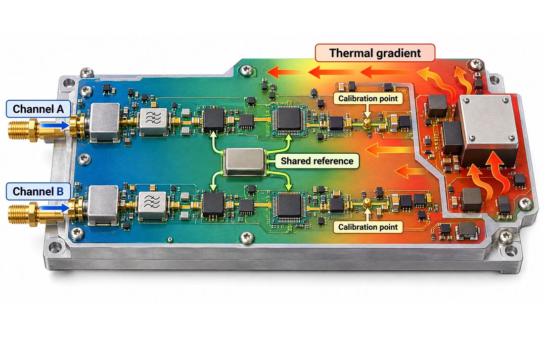
For a program illustration, imagine two receiver channels that pass nominal room-temperature testing but diverge after a thermal soak.
A useful engineering sequence is to log both path temperatures, repeat the same calibrated stimulus, compare phase and amplitude at a fixed reference plane, then swap only one controlled variable at a time. This is a proposed diagnostic workflow, not a KKPCB customer test or measured result. It gives an Aerospace PCB team a way to separate thermal imbalance from configuration drift without overstating what a bench observation proves. It can distinguish board asymmetry from oscillator behavior, connector repeatability, or a changed cable path.
Where a prototype is needed to validate assembly access and RF launch, a prototype assembly build should preserve the intended connector, shields, thermal interface, and reference clock parts. The build note should identify substitutions and calibration files. If connector bodies or shields are through-hole, document the connector soldering process and inspection criteria; board-side active devices may need a separate SMT assembly plan.
Make fabrication and release data support the analysis
A phase-sensitive release package should carry the controlled schematic, stackup, impedance notes, critical-path net names, connector and filter part numbers, reference-clock definition, calibration method, and approved test configuration. Tie each output to a revision. The Aerospace PCB release package should make the link from source design, fabrication drawing, assembly variant, and calibration file explicit. A changed laminate construction, surface finish, copper weight, connector footprint, or assembly substitution may alter the electrical delay or thermal environment; run an impact review before accepting the change as form-fit-function equivalent.
Ask the fabricator to review the finished board thickness, copper distribution, drill registration, layer transitions, trace geometry, and any special contact or carrier interface. If dense escape routing is unavoidable, consider whether HDI PCB routing can solve the fanout without compromising the critical RF channel; evaluate microvia reliability and the actual cross-section rather than assuming every fine-pitch escape is equivalent. For a board-to-board or harness architecture change, PCB assembly integration should review connector alignment, shielding, fastening, and rework access along with the bare-board drawing.
If enclosure packaging forces an interconnect to flex between a receiver and a remote antenna or service panel, evaluate a rigid-flex PCB architecture against a separate cable before committing the bend zone. Keep the RF launch and calibrated path outside any repeated-flex region unless the design and validation plan explicitly account for it.
Material substitutions deserve the same discipline. A different glass style or resin system can change dielectric behavior and therefore electrical length; a new solder mask or finish can affect local geometry and assembly. Record the approved material family and construction in the stackup, and require engineering approval before alternatives are used. For an Aerospace PCB, a material change should reopen electrical-delay and thermal-interface assumptions, not only the purchasing note. The Aerospace PCB package should describe the specific construction and acceptance evidence for this design rather than make a broad claim that any nominally similar laminate is interchangeable.
Release checklist for an RF navigation receiver
- Set system-level phase, amplitude, frequency, temperature, and recalibration requirements before assigning PCB tolerances.
- Separate clock stability, deterministic startup, RF-path delay, connector repeatability, and calibration residuals in the error budget.
- Compare the two channels across stackup, launches, vias, reference planes, copper environment, thermal sources, and carrier contact.
- Define the measurement plane, reference source, instrumentation uncertainty, sensor locations, thermal stabilization, and configuration record.
- Control laminate construction, copper, finish, connectors, filters, clock parts, assembly substitutions, and calibration data by revision.
- Run the program’s required qualification and assurance activities; this article does not imply aerospace approval, radiation tolerance, or completed testing.
A useful decision is not simply “make the traces equal.” It is to decide which phase terms the system must control, which the PCB can influence, and what evidence proves repeatability after fabrication and assembly. A documented RF receiver manufacturing review can then connect the layout assumptions to the released construction without presenting an engineering example as a completed customer result. The final Aerospace PCB review should close each requirement with an owner, controlled evidence, and a revision identifier. That keeps an Aerospace PCB phase claim tied to a defined configuration rather than a generic board-level promise.
Sources: Analog Devices, AD9361 product documentation and UG-570 reference manual (clock input, PLL reference, and phase-noise guidance); Analog Devices Wiki, AD9361 evaluation and multichip synchronization guidance; NASA Technical Reports Server publications on spacecraft RF phase stability and temperature-related phase coefficients. The AD9361 is cited as a public architecture example, not as an aerospace-qualified component. Apply the governing project specification and vendor revisions. The calculations above are analytical illustrations, not measured KKPCB data.





