
Multi-channel industrial measurement boards fail in a subtle way: every channel can look correct at room temperature, yet the readings drift when the converter warms, the cable bundle is moved, or the ADC reference shares return current with a field sensor. A dependable Industrial IoT PCB treats channel grouping, reference placement, thermal spreading, and calibration access as one system rather than as four independent layout tasks.
- Group sensor inputs by return-current behavior, not only by connector order.
- Keep the ADC reference and calibration point away from converter heat.
- Define the board datum and cable harness for repeatable thermal checks.
- Carry board, firmware, fixture, and sensor-lot revisions in the release record.
Partition the analog front end by function
Start with the sensor connector, protection, filter bank, amplifier, and ADC path. The PCB design should show where each channel returns and where the reference is measured. A connector pin order that is convenient for the harness can force a noisy excitation current beside a low-level channel. The Industrial IoT PCB stackup should give the analog region a stable reference while leaving enough copper for power and thermal spreading.
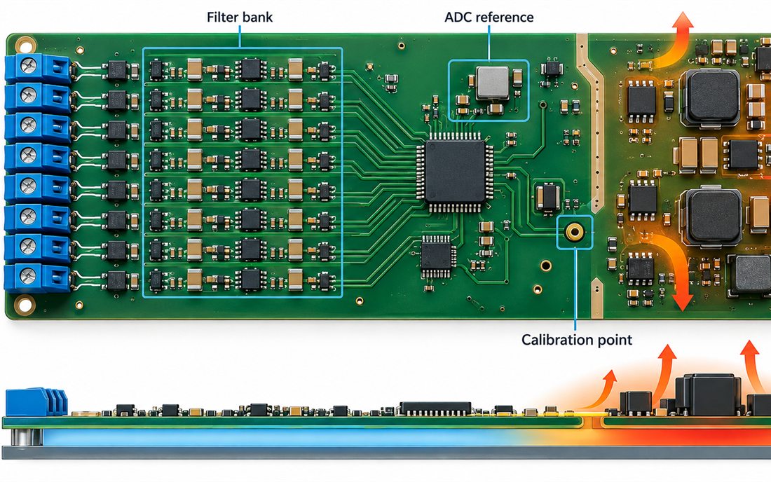
Place anti-alias components close enough to the ADC to control the intended loop, but preserve service access to the reference and calibration node. The PCB manufacturing drawing should identify copper balance and any via array that spreads converter heat toward the analog region.
Use thermal zoning to protect the reference
A converter or network processor can raise a local temperature without making the board feel hot to an operator. Keep the high-frequency PCB clock or network return compact, then separate it from the ADC reference and sensor return. If a copper spreader is needed, define whether it moves heat away from the sensor or toward it. Do not use a large pour as a substitute for an explicit heat path.
| Design region | Risk | Evidence to retain |
|---|---|---|
| Sensor inputs | Channel crosstalk or cable-current error | Connector map and return overlay |
| Filter bank | Placement or value change | Assembly drawing and BOM revision |
| ADC reference | Thermal or ground movement | Probe datum and calibration note |
| Power region | Heat or switching coupling | Stackup and copper-balance review |
The PCB assembly process can change thermal behavior through voiding, shield placement, solder coverage, or coating. Include the approved finish, component orientation, and any masked reference pad in the same release as the channel drawing.
Calibrate the board under a defined thermal condition
A calibration fixture should provide a reference source, controlled cable harness, board support, and a way to record the temperature at the board rather than at the chamber wall. The assembly fixture must locate the board by a repeatable datum and protect the sensor connector from accidental strain. A conceptual thermal-calibration setup is shown below; it is a method illustration, not a measured customer result.
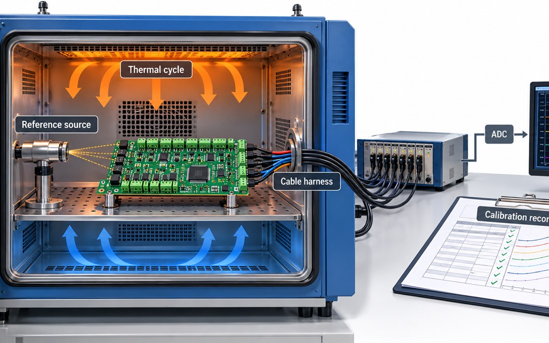
Record board revision, firmware revision, sensor lot, fixture revision, cable harness, and acceptance method. The PCB materials record should identify the approved laminate and coating because moisture or a substitute finish can shift the thermal response. The PCB fabrication traveler should keep the same identifiers after panel separation and cleaning.
Review changes that can move a channel
- Moving a converter, shield, connector, or thermal spreader.
- Changing a filter value, ADC reference, sensor lot, or cable harness.
- Changing stackup, copper weight, coating, or approved laminate.
- Changing firmware timing or the calibration fixture datum.
- Changing the enclosure airflow or mounting interface.
A production Industrial IoT PCB release needs more than a nominal channel schematic. The analog layout, the fabrication record, and the assembly traveler should point to the same calibration fixture and board datum.
The project manager should receive a signed handoff that distinguishes design targets, typical material values, and production measurements. Procurement can then approve the approved material and return-path rule without losing the context of the analog measurement.
The Industrial IoT PCB material record should stay with the channel map, and the Industrial IoT PCB layout should preserve the thermal boundary after a component ECO.
Freeze the analog thermal assumptions
For an Industrial IoT PCB, the Industrial IoT PCB channel map should name the sensor lot, filter revision, and ADC reference. If an Industrial IoT PCB moves the converter, review the thermal path before recalibration. If an Industrial IoT PCB changes its enclosure, repeat the airflow check. The Industrial IoT PCB fixture should keep the cable harness and board datum constant. A production Industrial IoT PCB record should distinguish a design target from a measured result.
The Industrial IoT PCB release owner should keep the Industrial IoT PCB layout, Industrial IoT PCB material record, and Industrial IoT PCB calibration fixture on one revision-controlled traveler.
At pilot release, the calibration owner should state the reference condition, warm-up sequence, cable harness, firmware revision, and board support points.
The operator should see the sensor connector, probe datum, and ADC reference without removing a shield or flexing the board. If the board is coated, mark the masked reference pad and sensor interface before the first lot.
If the board is panelized, keep the same orientation in the thermal fixture so one channel is not consistently closer to a heat source.
These notes are not a substitute for a qualification report. They are the manufacturing evidence needed to explain a drift complaint. The project manager can separate a component-lot effect from a layout change, enclosure change, or fixture change, and assign the next action to the correct team.
The Industrial IoT PCB owner should sign the Industrial IoT PCB channel map against the fixture datum. The Industrial IoT PCB traveler then carries the same board and sensor-lot identifiers into production.
Industrial IoT PCB channel release
Release the Industrial IoT PCB channel map with the thermal and calibration assumptions visible to production.
An Industrial IoT PCB inspection image should show the board datum and calibration access after assembly.
Sources: Analog Devices precision signal-chain and power-integrity guidance; Würth Elektronik grounding and assembly notes; Qorvo interface references; sensor, ADC, converter, cable, coating, and PCB material supplier application data. Checks above are engineering practices or design targets, not customer measurements.wbu’s
