
Table of Contents
A door sensor or room monitor can meet its firmware sleep target and still miss the product battery-life promise. Connector leakage, regulator quiescent current, radio bursts, sensor warm-up, and a narrow return path can consume the margin that a spreadsheet never sees. A dependable Smart Home PCB exposes the energy path and gives manufacturing a repeatable way to verify it.
Why the battery budget becomes a PCB problem
Average current hides the events that damage a small battery node. A radio burst can pull down the rail, a sensor can sample before its reference settles, and a disabled peripheral can remain powered through an I/O pin. The first Smart Home PCB review should list sleep current, wake current, settling time, load-switch state, battery impedance, and the return path for each domain.
Start at the battery connector and follow current through protection, regulation, load switching, sensor excitation, processor, and radio. A power-tree map makes the trace width, via count, decoupling location, and connector contact meaningful. When a regulator alternate or coin-cell holder changes, the map tells the team which transient and leakage checks must be repeated.
Thermal behavior still matters in a low-power design. A regulator that is cool in sleep can heat the sensor or enclosure during a burst or charging event. Keep the power loop compact, provide copper for heat spreading, and prevent that copper from becoming an unintended antenna counterpoise. For a released Smart Home PCB, freeze the battery, regulator, and RF stackup assumptions together.
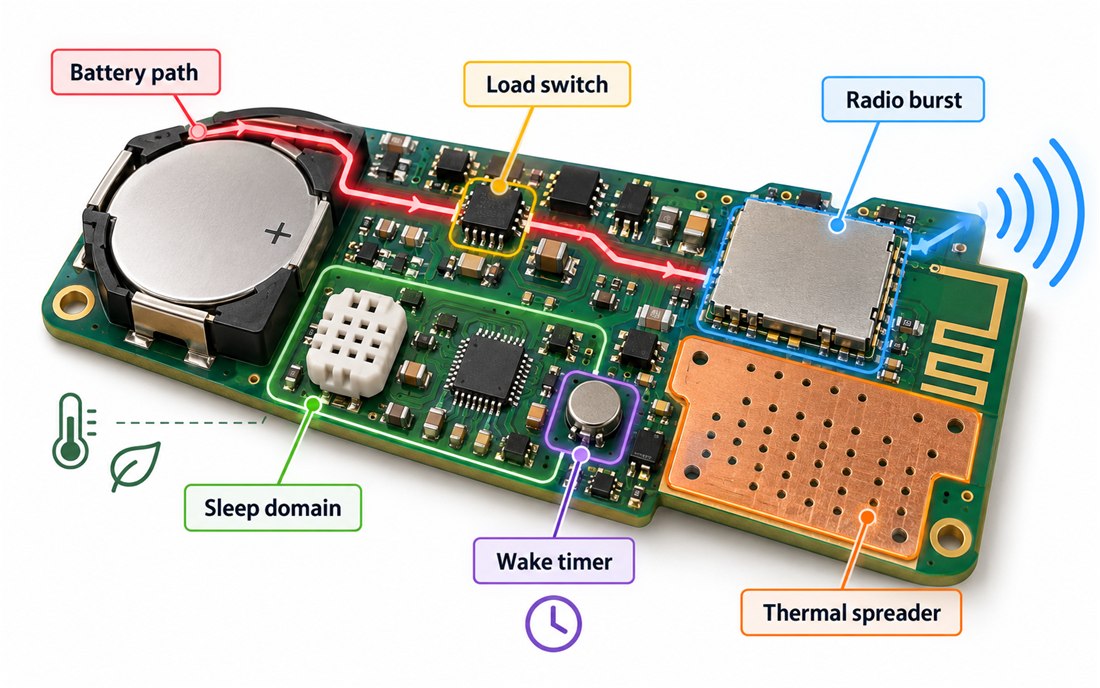
This conceptual image shows battery path, load switch, sleep domain, wake timer, radio burst, and thermal spreader. It is a design explanation, not a measured current trace. Use a power-release checklist to connect the schematic assumptions to the actual copper, vias, and assembly inspection points.
Partition sleep, sensor, and radio domains
A clean partition starts with states, not colors on a layout. Define what is powered in deep sleep, what wakes first, which signal enables the next domain, and where every off-state current can flow. A sleep-domain boundary should include the return path and the protection strategy, not only a load-switch symbol.
Keep the sensor reference and first decoupling close to the device. Keep processor and radio burst current out of the narrow neck that feeds the analog section. A decoupling placement review should confirm pad geometry, solder access, polarity, and the support condition used during rework.
Do not let an enclosure screw, flex cable, or programming header bridge a quiet domain into a switching loop. A return-path inspection should verify that the released board matches the intended partition after panelization and depanelization.
Measure wake behavior without loading the node
Low-power validation is a timing problem. Record the sleep interval, sensor wake, settling window, ADC sample, radio burst, and return to sleep. A battery-test fixture should locate the board, connector, enclosure, and current-shunt access without adding a long probe lead or changing the antenna condition.
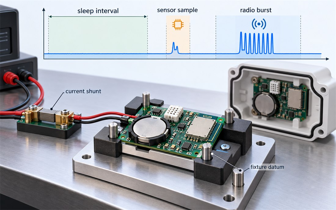
The second conceptual image shows sleep interval, sensor sample, radio burst, current shunt, and fixture datum. The timeline is illustrative and contains no measured values. Use a wake-timing record to capture firmware build, supply condition, sensor stimulus, board revision, and enclosure state with each comparison.
Separate average energy from transient integrity. A Smart Home PCB node can have a good average number and still lose data when the rail dips during a burst. A fixture-configuration log helps the project manager determine whether a change came from the board, battery, firmware, radio module, or test setup.
Release a low-power node for production
Release documents should include the battery holder drawing, power-tree map, off-state table, load-switch part, decoupling limits, current-shunt position, fixture datum, and acceptance method. A low-power assembly traveler and process-window record should call out connector seating, polarity, solder coverage, and any rework limit that can change leakage.
- Define sleep and wake states at schematic, layout, firmware, and test levels.
- Keep radio burst current away from the sensor reference and quiet return.
- Expose current-shunt and probe access without changing the enclosure or antenna.
- Repeat the timing check after regulator, sensor, battery, or firmware changes.
- Record board revision, fixture revision, and approved component lots.
The production Smart Home PCB should make battery behavior explainable. When the board, firmware, fixture, and enclosure share one release definition, a range or life complaint can be traced to a specific energy path instead of guessed from a single current number.
What to hand to the firmware and test teams
For a Smart Home PCB that wakes a sensor and then transmits a short packet, the release package should name the sleep current budget, the wake timer tolerance, the regulator settling assumption, and the radio burst window. A second Smart Home PCB revision is not equivalent if a pull-up, status LED, or protection device changes the quiescent path. Put those assumptions beside the assembly drawing so the firmware team can compare its duty cycle with the electrical design.
During pilot build, reserve one controlled access point for the current shunt and one probe point for the radio supply. This gives the line a repeatable way to separate battery chemistry, regulator loss, and radio demand without treating a single oscilloscope capture as a customer measurement. That distinction keeps the Smart Home PCB review honest while still giving engineering a practical pass/fail method.
Before sign-off, the Smart Home PCB checklist should include the battery connector, the enclosure ground interface, and the radio keep-out. A clear owner for each item prevents a late Smart Home PCB ECO from silently changing the energy budget.
Sources: Analog Devices low-power mixed-signal and power-integrity guidance; Würth Elektronik power, EMC, and assembly notes; Qorvo wireless-burst integration references; battery, regulator, sensor, and connector supplier data. Values above are engineering practices or design targets, not customer measurements.
