
Table of Contents
A Zigbee PCB can pass a clean-room range check and still drift after humidity exposure, aqueous cleaning, or conformal coating. Engineers often look first at firmware or the radio IC, yet the change may come from absorbed moisture, ionic residue, a coating meniscus, or an enclosure seal that moves the antenna boundary. This article addresses the project pain point: how to keep a short-range wireless board stable when environmental processing is part of the manufacturing route.
Why a stable radio drifts after environmental processing
The RF network is sensitive to the geometry and dielectric material immediately around the antenna. A Zigbee PCB does not need a high microwave data rate to show this effect; a compact inverted-F, meander, or chip antenna still depends on a repeatable reference plane, clearance, and enclosure relationship. Moisture can change the effective dielectric environment. Cleaning residue can create a conductive film near the feed. Coating can add a local layer that was not present when the matching network was tuned.
For a Zigbee PCB program, the first project decision is to separate three possible causes: board material response, process contamination, and mechanical enclosure change. Measure or inspect them as separate gates. If all three are changed between prototype and pilot build, a range comparison cannot identify the root cause. A controlled RF layout release therefore freezes the antenna outline, ground cutback, component orientation, coating boundary, and enclosure datum before the environmental process is approved.
Use a risk table rather than a generic “environmental test passed” statement. For a Zigbee PCB release, record whether the board is cleaned, baked, coated, or sealed; which surfaces are exposed; and whether the antenna is inside or outside the coating mask. This gives a project manager a traceable change record when field units show intermittent pairing or reduced range.
Control moisture, residues, and the antenna boundary
Material and moisture handling
Published laminate data should guide the material decision, but the assembly route still controls the final condition of the board. Store and condition panels consistently, avoid an uncontrolled delay between cleaning and coating, and define the time allowed before the enclosure is closed. The objective is not to claim a universal moisture value; it is to make the state of each Zigbee PCB comparable when RF verification begins.
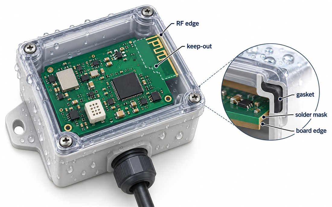
For the fabrication package, identify the antenna keep-out on the copper, solder mask, and assembly drawings. On a Zigbee PCB, the keep-out must cover the actual board edge, not only the copper pattern. A seal, adhesive bead, or coating dam that intrudes into the area can become part of the antenna system. A practical RF keep-out note should state what is prohibited, what is conditionally allowed, and how the boundary is inspected.
Cleaning residues are an RF and reliability issue
Cleaning should be released with both visual and process evidence. Flux residue, detergent film, and trapped moisture under a component can create a leakage path or alter the local surface condition. Inspect the antenna edge, matching components, connector pads, and test points with the same lighting and magnification used for the first article. A cleanliness inspection plan should distinguish visible residue from ionic cleanliness evidence rather than treating them as interchangeable.
Do not allow a last-minute cleaning change to bypass RF review. A new chemistry, rinse temperature, or drying step can change the surface energy and the amount of liquid held at the board edge. If the process must change, compare the antenna region before and after cleaning and confirm that the matching network is still accessible for debug. This is especially important for a Zigbee PCB that will be tuned inside a narrow enclosure.
Design the conformal-coating process around RF and test access
Mask the antenna without creating a new edge
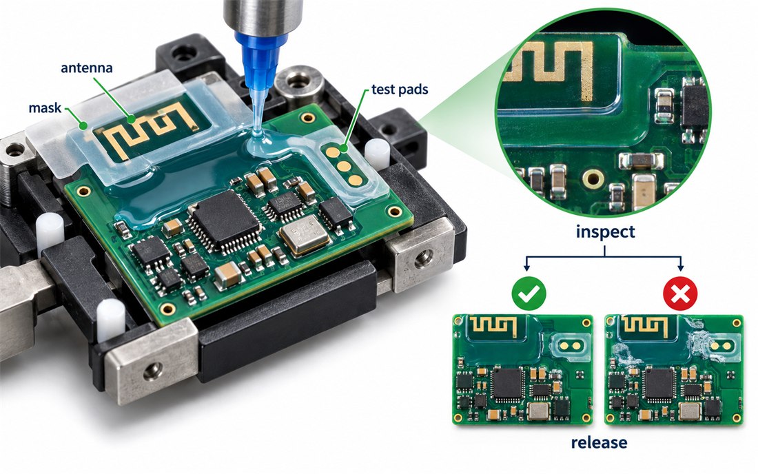
For a Zigbee PCB, conformal coating is not automatically harmful to RF performance, but an uncontrolled coating edge is difficult to reproduce. Define the mask line from the antenna geometry, keep the spray or dispense path away from the feed and matching components, and specify whether the board edge itself is coated. The mask must also preserve the connector and programming interface used during production test.
A controlled conformal coating process should include fixture orientation, spray direction, cure condition, and inspection points. It should not rely on an operator’s visual memory. Use a board drawing with the antenna, test pads, and no-coating regions highlighted. If the coating is selectively applied, check for a meniscus or pooled material that reaches the RF edge.
Some products require the antenna to remain uncoated while the rest of the board receives protection. That decision must be reviewed with the enclosure, gasket, and cleaning teams. A coating boundary that is safe in open air may be too close after the board is compressed into a plastic housing. The correct antenna matching review therefore uses the final mechanical datum and the final coating mask, not a bare-board photograph.
Keep production test repeatable
RF verification is most useful when the fixture sees the same board state every time. Define the board support points, connector datum, antenna orientation, and the time between coating cure and test. A test fixture that presses on the antenna edge or changes the enclosure position can hide a coating problem or create one. Keep the fixture contact map in the assembly release package.
For a product manager, the important question is not whether one sample paired successfully. It is whether the process can identify a drift before shipment. Set an acceptance method that compares the same channel plan, enclosure state, and firmware build. Record a target or engineering reference range only when it is supported by the project specification; otherwise, use comparative checks and document the limitation.
Release evidence for production and field support
A production-ready Zigbee PCB should carry one environmental release package: material and storage condition, cleaning route, coating mask, cure and inspection method, antenna boundary, test fixture datum, and change-control owner. The package should make it obvious which variable is allowed to move and which variable requires RF approval.
Before pilot release, confirm the solder mask boundary, humidity cycling, DFM release, surface finish, and production change control. These five business checks are separate from the five core-keyword links, but together they give engineering, manufacturing, and program teams a common release language.
A useful field-return review compares the returned board with the approved coating and enclosure state. Inspect the antenna edge for residue, check connector seating, review the cleaning and cure records, and then decide whether the issue belongs to RF tuning, process control, or mechanical sealing. That sequence prevents a firmware workaround from masking a repeatable PCB process problem.
Sources: Published laminate material data and handling guidance; Analog Devices RF layout and grounding resources; Qorvo antenna and front-end application material; Würth Elektronik PCB manufacturing and reliability notes; KKPCB internal RF, assembly, and DFM release practices.
