
Table of Contents
A Zigbee PCB can pass a single-board layout review and still lose repeatability when it enters a manufacturing panel. Breakaway rails, tooling holes, router paths, copper balance, and depanelization forces can move the RF edge or leave residue beside the antenna. The failure often appears as a range complaint, but the project root cause is a release package that never treated the panel as part of the radio design. This guide gives engineers and project managers a practical way to keep a Zigbee PCB electrically stable after it becomes a production array.
Treat the panel as an RF state, not only a manufacturing drawing
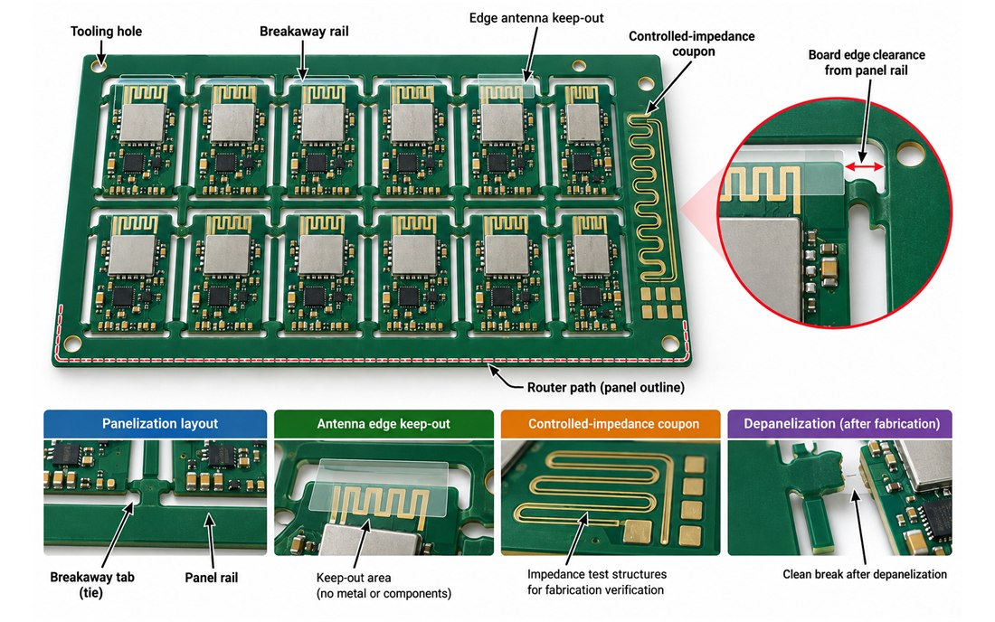
Start the review by showing the separated board, the complete array, and the final carrier or pallet. On a Zigbee PCB, the antenna edge, the first ground reference, the feed transition, and the nearest copper must remain visible in all three views. A rail can behave like a metal wall beside a printed antenna; a tooling hole can force a keep-out change; and a tab can leave glass-fibre or copper residue at the very edge that was tuned in the CAD file.
The project team should freeze one panel datum before routing begins. Record the board origin, array pitch, rail width, tooling-hole pattern, fiducials, and the board edge used for the RF reference. If the assembler later changes the carrier, the change should return to the RF owner for review rather than being treated as a harmless production adjustment. This simple change-control rule prevents a late panel edit from silently changing the antenna environment. It also gives each Zigbee PCB revision a traceable panel baseline.
For a practical Zigbee PCB review, compare the isolated board against the panelized Gerber or ODB++ view. Confirm that no copper pour, copper thieving pattern, breakaway tab, or temporary support enters the antenna keep-out. The same review should verify that the feed line still sees a continuous return path and that the panel rail does not create an unintended resonant metal feature.
Protect the antenna edge, feed, and return path
Separate RF geometry from breakaway mechanics
Place breakaway tabs in low-current, low-stress regions. Do not put a tab through the antenna current path, below a chip antenna ground clearance, or beside a board-edge connector that must remain square after singulation. When a tab must be close to the radio edge, define a minimum distance in the fabrication drawing and show the distance on the panel drawing, not only in a schematic note. A clear Zigbee PCB and stackup callout also keeps the dielectric thickness from changing while the mechanical team is adjusting the array.
Keep the first ground reference continuous beneath the feed. A common mistake is to remove copper from the separated board but restore a copper rail in the panel to improve plating balance. That rail can couple to the feed during electrical test and can make a good board look bad only while it is still attached to the array. Use a local copper-balance rule outside the RF boundary, and document the boundary with a dimensioned drawing.
Use a panel-aware impedance check
For a controlled feed, the design review should carry the line width, dielectric height, copper thickness, and reference plane into the panel data. If the panel changes the local copper density, request a short coupon or a representative first-article check rather than assuming the isolated-board value survives unchanged. The coupon does not need to claim a customer measurement; it is a release tool that lets the team compare the approved geometry with the fabricated geometry.
During controlled impedance planning, define which features are allowed to move and which are not. A rail can move by a routing tolerance, but the antenna edge and the feed datum should have a tighter, explicitly reviewed tolerance. This distinction gives the manufacturer room to panelize without turning the RF boundary into an uncontrolled variable.
Control tabs, rails, routing and depanelization
Mechanical release should treat the panel as a sequence of forces. V-score applies a bending moment along a line; routed tabs concentrate force at small bridges; and a manual snap can pull solder joints or crack a ceramic component. For a small Zigbee node, the resulting defect may be microscopic but still change antenna clearance or connector seating. The panel drawing should identify the intended separation method, the tool direction, the maximum unsupported span, and the edge-cleaning method. For a Zigbee PCB, this mechanical sequence should be reviewed alongside the RF boundary.
For the PCB manufacturing team, a robust panel includes a rail wide enough for tooling and inspection, fiducials with a clear camera field, and copper balance that does not invade the RF boundary. For the PCB assembly team, the same array must present a stable support surface under the antenna and connector. These requirements should be reconciled before the stencil and program are released.
Do not hide the panel risk in a generic DFM note. Mark the antenna edge, the keep-out, the tab locations, and the no-clamp zones in the same release package. If a project manager sees a panel change late in the schedule, the decision can then be made against visible constraints instead of a debate about whether a rail is “far enough away.”
Inspection after singulation
First-article inspection should compare a separated board with the approved outline. Check edge profile, burrs, resin exposure, copper nicks, and residue near the antenna. Measure the connector datum and inspect the solder mask boundary against the RF keep-out. A board can be mechanically acceptable yet electrically different if a thin copper sliver remains beside the antenna. Capture photographs against a simple overlay so the evidence can be reviewed at the next build.
Use assembly inspection and design release as linked checkpoints, not as separate departments. The first article is the point where the CAD owner, the manufacturer, and the assembler can still correct the panel without scrapping a full lot.
Release evidence for assembly, test and field support
A panelized Zigbee PCB should ship with a compact evidence package: approved stackup, panel drawing, antenna keep-out, depanelization method, controlled-feed coupon definition, first-article photographs, and the sign-off list. This package is more valuable than a long generic checklist because it connects each manufacturing feature to the RF behavior that matters in the product. It gives the next Zigbee PCB revision a repeatable release baseline.
For production handoff, tie the array revision to the BOM and assembly program. If the antenna vendor, connector, solder mask, or board outline changes, require a panel review even when the schematic is unchanged. A project manager can then distinguish a cosmetic change from a change that may alter range, coexistence, or enclosure fit.
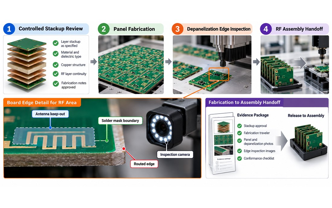
Before release, confirm the panelization drawing, antenna keep-out, ground return, depanelization method, and first-article evidence. These five checks make the handoff auditable without pretending that a conceptual drawing is a measured customer result. They keep every Zigbee PCB release tied to a visible manufacturing decision.
Sources: Taconic RF laminate application notes and published material data; Analog Devices RF layout guidance; Qorvo antenna and front-end design resources; Würth Elektronik RF and PCB manufacturing notes; KKPCB internal DFM and RF release review practices.
