
The released Megtron 6 PCB construction is the reference for the DFM package. Any supplier change to a Megtron 6 PCB must carry the same stackup and coupon revision, so procurement can compare capacity without changing electrical intent.
Megtron 6 PCB DFM release work is where a high-speed design becomes a repeatable production definition. A stackup can meet an impedance target in simulation and still create yield risk when resin content, copper balance, drill compensation, registration, panelization, and inspection datums are not frozen together. This guide focuses on checks that help engineers, buyers, and project managers release a manufacturable board without inventing customer test results.
Table of Contents
- Convert intent into a controlled stackup
- Review fabrication and panel constraints
- Build the evidence package
- Release checklist
Convert the electrical intent into a controlled build
A Megtron 6 PCB release should start with one controlled stackup that names the exact material grade, glass style, finished dielectric thickness, copper range, surface finish, and impedance method. Panasonic MEGTRON 6 family data provides typical Dk, Df, Tg, Td, CTE, and thermal values for specific constructions; use those values as engineering inputs, not as a blanket guarantee for every pressed board.
For each high-speed pair, record the reference planes, target impedance, tolerance, allowable skew, and transition type. If the design includes a thin core, sequential lamination, back-drill, or a large connector field, show those features in the same release table. The PCB layout review is complete only when the layer map, mechanical datum, and SI assumptions agree.
Review fabrication constraints before CAM release
Registration, copper balance, and drill strategy
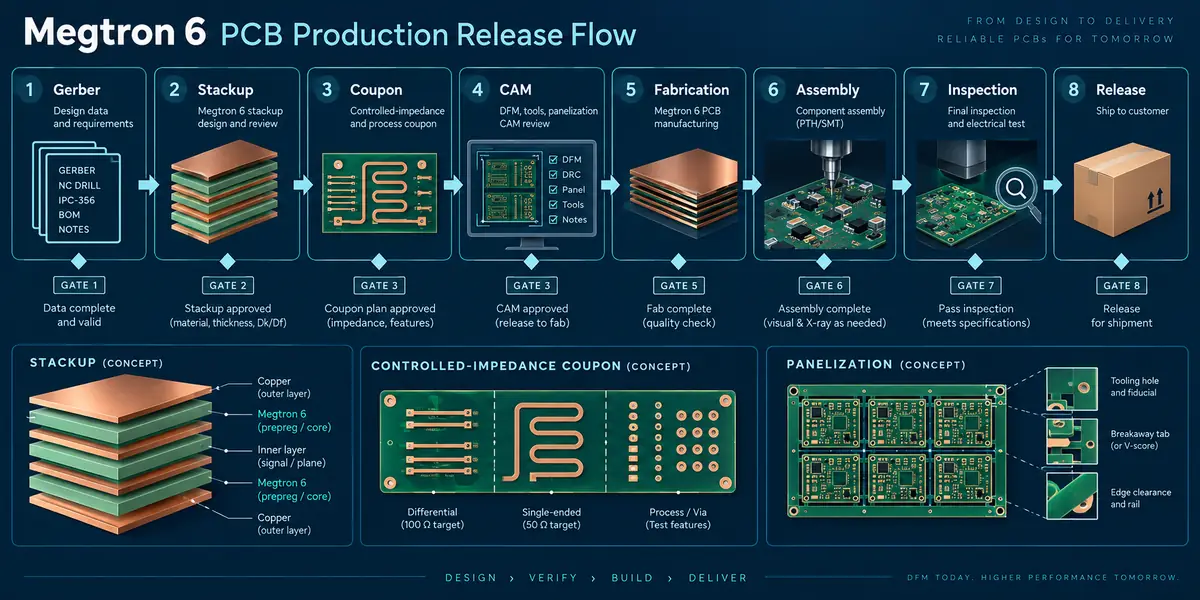
Dense copper on one side of a panel can change press behavior and plating distribution. Large plane areas, narrow neck-downs, and connector breakouts should be reviewed by layer and by panel quadrant. The high-speed PCB manufacturing handoff should state the finished copper range, etch compensation, drill tolerance, plating requirement, and back-drill datum. Do not leave those values in an email disconnected from the released drawing.
Registration-sensitive features need nearby targets and an inspection method. A generic edge coupon may not represent the product’s densest BGA, via field, or connector launch. For the selected construction, place coupons where the dielectric, copper pattern, and drill structure consume the same process window as the product. If a supplier changes the press construction or foil type, route it through engineering change control.
Make the evidence package useful to production
The release package should let CAM, fabrication, assembly, and inspection teams answer the same questions. Include the stackup, impedance table, coupon drawing, drill chart, panel array, copper-balance note, surface-finish callout, and cross-section request. The Megtron 6 materials reference identifies the family, while the build drawing defines the actual product construction.
For early programs, PCB prototype assembly can reveal connector fit, paste constraints, reflow support, and inspection access. Treat those findings as design inputs for production rather than proof that a later panel will behave identically. A new connector, solder-mask opening, finish, or panel array can move the electrical and mechanical datum.
Coordinate assembly, inspection, and change control
Assembly constraints belong in the same release logic. Paste apertures, mask expansion, component keep-outs, connector coplanarity, and board support can affect the launch and reference-plane return. The PCB assembly review should use the same critical datums as fabrication and SI. The PCB materials decision, if a dedicated page is available, should never replace the exact stackup note in the purchase package.
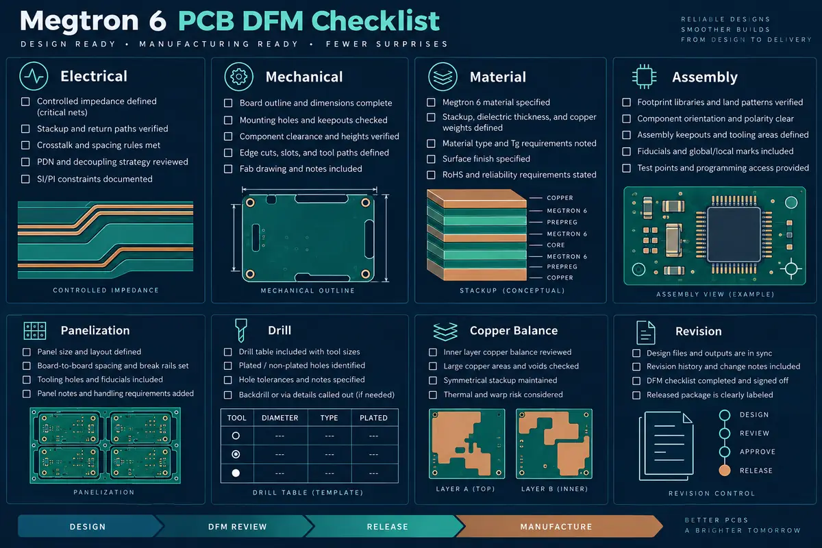
Production release checklist
- Exact grade, glass style, finished dielectric, copper range, finish, and test method named.
- Impedance, skew, loss, drill, registration, and panel tolerances separated into targets and acceptance limits.
- Panelization, copper balance, tooling holes, coupons, and inspection datums reviewed together.
- Back-drill, via, connector-launch, mask, paste, and assembly keep-outs shown on controlled drawings.
- Cross-section method and evidence package defined before the purchase order.
- Supplier substitutions, CAM deviations, and assembly changes routed through formal change control.
For a project manager, the final Megtron 6 PCB DFM release is ready when design intent, fabrication capability, assembly constraints, and inspection evidence are traceable to one revision. The final Megtron 6 PCB package should make the production decision easy to audit and repeat.
For a first-article build, the release owner should map each critical feature to one piece of evidence: stackup and impedance review for electrical intent, cross-section for pressed thickness and copper, dimensional inspection for registration, and assembly inspection for connector and mask conditions. This avoids a common handoff failure in which fabrication signs off a drawing while assembly is still working from an earlier keep-out or finish note.
When a Megtron 6 PCB supplier proposes a material, foil, or panelization change, compare the change against the same lane, via, coupon, and inspection assumptions. A lower-risk approval records the affected drawing revision, the expected process benefit, and the verification step that will close the change. That record gives purchasing a clear decision path without turning an unverified substitution into a production fact.
Panel-level decisions deserve the same discipline. Keep tooling, breakaway, copper thieving, and coupon locations visible on the array drawing, then review the most copper-dense and least copper-dense quadrants. If the product includes a large connector field or back-drilled vias, the panel review should show how those features are supported during lamination, drilling, plating, and inspection. The goal is not a generic capability statement; it is a release package that another team can interpret without guessing.
Before purchase order release, freeze the acceptance vocabulary as well: target, tolerance, inspection method, sample size, and change approver. That small discipline makes a DFM review useful to both engineering and operations.
Keep that vocabulary in the purchase package so every Megtron 6 PCB release can be compared against the approved baseline.
The same Megtron 6 PCB baseline should govern the pilot build, supplier review, and later production change.
Sources: Panasonic Industrial Devices MEGTRON 6 family and R-5775/R-5670 technical data; supporting DFM, high-speed layout, and RF assembly guidance from Analog Devices and Qorvo application material; KKPCB verified pages for manufacturing, layout, assembly, prototype assembly, and MEGTRON 6 material capability. Values are typical or design-reference values unless a released drawing defines the acceptance limit.
