
GNSS receivers and compact radar modules bring incompatible noise budgets onto the same board. The RF path needs a quiet reference and controlled geometry; the digital processor needs clocks, memory, and power conversion; the project team needs all of it to fit a repeatable stackup. A Taconic TLY-5 PCB mixed-signal layout succeeds when return current is planned at the same time as signal routing. Splitting copper after routing usually moves the problem into a connector, a via transition, or a power island.
Separate RF, clock, power, and digital return paths
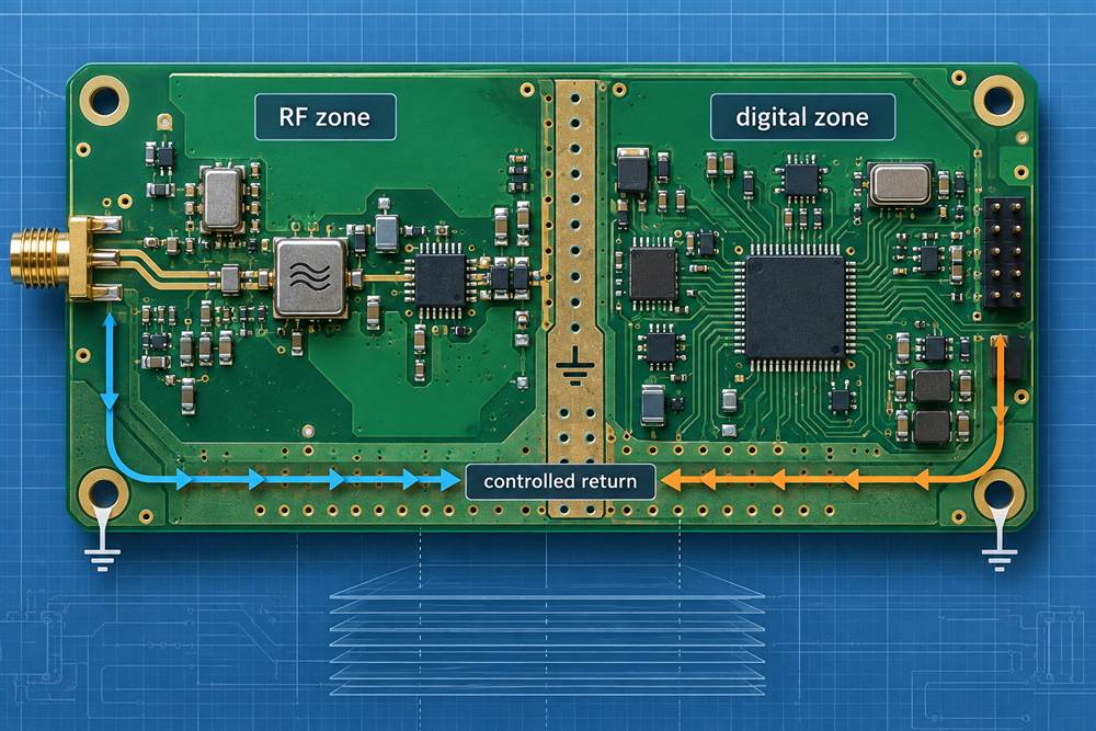
Begin with a partition that follows current, not only component function. Put the antenna feed, low-noise amplifier, and filter chain in a compact RF zone; place the clock source and fast digital interfaces where their reference planes remain continuous; keep switching regulators away from the receive aperture. For a Taconic TLY-5 PCB, the laminate data helps establish the RF model, but the return path still depends on layer pairing, plane width, stitching, and the placement of connectors and mounting hardware.
A useful review marks the forward path and the return path in different colors. If a clock crosses a plane split, identify the capacitor or stitching bridge that provides its return. If an RF trace changes layers, show the ground vias that carry the displacement current. This markup gives a project manager a concrete way to ask whether a late component move changes the electrical boundary.
Select layer transitions that preserve reference continuity
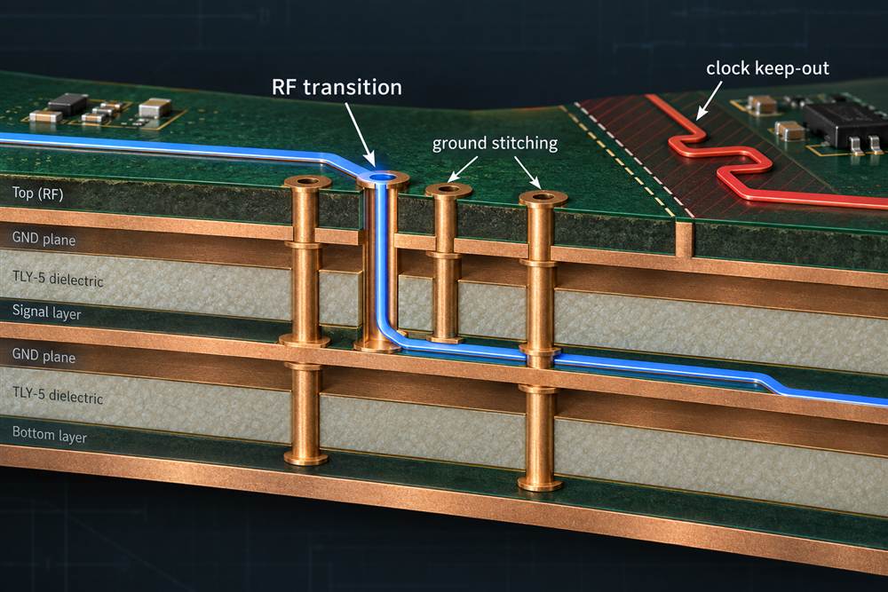
A Taconic TLY-5 PCB radar or GNSS feed should not be routed through a transition simply because the via is available. Define the signal via, antipad, back-drill rule, and nearby ground vias as one transition cell. Keep the reference plane close enough to control field spread, and avoid placing a power void under a sensitive launch.
Use controlled-impedance PCB rules for the RF net class, then add mixed-signal constraints for clock length, edge rate, and aggressor spacing. The RF transition model should include the actual mask condition and the copper treatment expected after fabrication. A nominal trace width is not a complete requirement if etch compensation, resin distribution, or registration can change the effective geometry.
Transition review questions
-
- Does every signal via have a low-inductance ground return?
- Does the antipad preserve the intended field shape through each reference plane?
- Can drilling and back-drilling hold the specified depth across the panel?
- Are clock and RF transitions kept away from the antenna aperture and connector keep-out?
Protect GNSS and radar interfaces during assembly
After layout, the PCB manufacturing drawing must preserve the partition. Show copper keep-outs, mask openings, via fences, shield lands, and the mechanical datums used for antenna alignment. Avoid adding a large copper pour late in the process without checking whether it changes the RF reference or panel balance.
At assembly, protect the EMI shielding GNSS antenna feed and radar launch from paste spread, shield-solder bridges, and connector coplanarity issues. A PCB assembly traveler should identify the RF-sensitive pads, the acceptable reflow window, cleaning restrictions, and the inspection view used after shield installation. If a shield can is reworked, record the change and recheck the keep-out; a mechanical repair can become an RF boundary change.
Release a mixed-signal verification plan
Use a product-correlated coupon for the most sensitive RF layer pair and transition. The coupon should carry the same dielectric construction, copper treatment, and via style as the GNSS or radar feed. Record design targets separately from measured results. A supplier’s typical Dk or Df value is an input to the model; it is not evidence that a finished channel has been measured.
During first article review, inspect registration between the RF trace and reference plane, via position, mask edge, shield land, and connector datum. If the board uses a Taconic TLY-5 PCB mixed-signal stackup, keep the RF layer and digital return map in the same controlled revision. A change to power-plane shape, clock escape, or mounting-hole copper should be evaluated for both EMI and phase impact.
GNSS and radar handoff checklist
- Partition zones by current and return path before final placement.
- Document every RF and clock transition with its reference-plane strategy.
- Keep assembly pads, shields, and cleaning rules out of the RF aperture.
- Correlate coupons and inspection views with the product geometry.
- Reopen the return-path review after any material, plane, or connector change.
With those controls, a Taconic TLY-5 PCB can support GNSS and radar functions on one mixed-signal platform without relying on hidden copper fixes. The objective is a return-path plan that remains understandable to design, manufacturing, assembly, and test teams.
Before procurement, the Taconic TLY-5 PCB return-path map should be checked against the Taconic TLY-5 PCB stackup and the Taconic TLY-5 PCB connector locations. Keep the Taconic TLY-5 PCB change record with the RF review so a plane or clock move is not missed.
Sources: AGC public TLY-5 material data; Analog Devices mixed-signal layout guidance; Qorvo RF front-end practices; KKPCB RF stackup, manufacturing, and assembly release methods reviewed for this article.
