
Dense wireless modules often pass an electrical review and still show channel-to-channel coupling after the first hardware build. The cause is usually not one missing via; it is an incomplete return path around a connector, a layer transition, a shield edge, or a digital escape. A Taconic TLY-5 PCB via-fence design should therefore be treated as a current-management system. The fence must contain the field, connect to the intended reference plane, and remain possible to drill, plate, inspect, and assemble.
Locate the coupling path before placing vias
Start by marking the source, victim, and return path for every sensitive interface. On a Ku-band front end, the source may be an edge-launch trace or a power-amplifier output; the victim may be a receive line, clock trace, or adjacent antenna feed. A fence added at the wrong layer can look dense in a top view while leaving the actual return current to spread through a plane void.
For a Taconic TLY-5 PCB, freeze the dielectric height and copper reference before selecting a via pitch. Public TLY-5 data is useful for the first field model, but effective coupling still depends on finished trace width, solder-mask boundary, plated barrel, and the distance from the RF edge to the nearest reference via. Put those assumptions on the stackup drawing so the RF designer and fabricator are not working from different baselines.
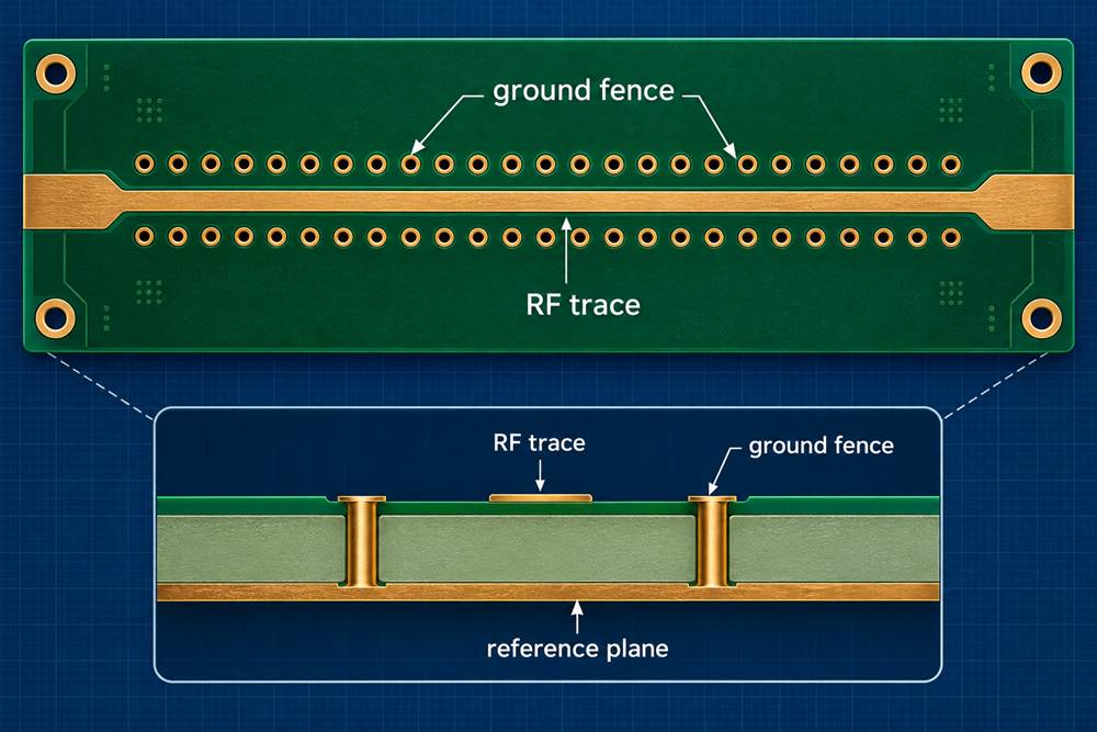
Build a repeatable fence and reference transition
Use Taconic TLY-5 PCB design rules to keep the fence tied to the same reference plane used by the trace. Define via diameter, finished hole, pad, antipad, center-to-center pitch, and edge offset. A fence that is electrically continuous but mechanically too close to a connector can force a late footprint change. A fence that is too far away can leave an open coupling window. The correct pitch is the one supported by the frequency, geometry, and fabrication window—not a copied rule of thumb.
Keep the fence path free of plane splits. If a trace changes layers, provide a short, low-inductance return transition with ground vias near the signal vias. A controlled-impedance PCB review should show the current path in cross-section, not only the top copper. Mark back-drill requirements, via-in-pad restrictions, and any buried or blind-via assumption before the board reaches quotation.
Four checks before routing is frozen
- Identify the victim net and its nearest reference plane on every layer.
- Show where return current crosses a signal-via transition.
- Check that the fence does not block connector seating or inspection.
- Confirm the pitch and edge clearance can be drilled and plated across the panel.
Coordinate shields, connectors, and assembly access
A shield wall changes the field only when its ground connection is low inductance and continuous. Connect shield pads to a planned via row, then verify that the row lands on the same ground system as the RF launch. Avoid a decorative ring that connects through long necks or isolated copper islands. The PCB manufacturing drawing should identify the keep-out, solder-mask opening, and plating condition at the shield interface.
Connector transitions need the same discipline. A RF connector launch should preserve the launch pad, antipad, and ground-via relationship used in the model. Leave assembly access around the connector so the operator can inspect the solder fillet and the via row after reflow. If a shield can is installed late, reserve the land pattern and cleaning path before routing digital escape traces.
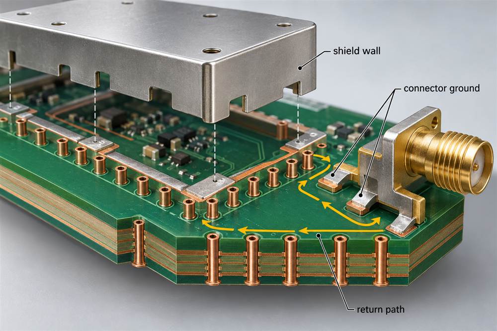
Verify the fence in DFM and first article release
For multilayer products, the multilayer PCB stackup and the via-fence map should be released together. Ask the fabricator to check registration between the RF layer, reference plane, and ground-via row. If the fence is close to a board edge, panel rails and routing holes can change the local copper balance; panelization should preserve the same boundary on every repeated unit.
During first article inspection, verify via location, finished hole, annular ring, mask clearance, and continuity to the intended plane. Use a coupon only when it represents the same layer pair and via construction. Do not claim measured isolation from a conceptual layout. Instead, define the design target, the inspection method, and the decision if a via shifts outside tolerance.
A populated Taconic TLY-5 PCB build also needs an PCB assembly check. Confirm that paste, shield installation, wash, and rework do not bridge the fence or cover a test pad. When the fence is part of an RF module, a change to pad opening or shield height should trigger an RF review rather than a silent assembly adjustment.
Release checklist
- Return-path markup exists for every RF layer transition.
- Via pitch, drill, plating, and mask limits are on the drawing.
- Connector and shield access remains inspectable after assembly.
- Coupon geometry correlates to the product’s most sensitive fence.
- Any stackup, shield, or via substitution has a documented change gate.
When those controls are linked, a Taconic TLY-5 PCB can contain coupling without turning every revision into a tuning exercise. The engineering value is not a visually dense via row; it is a reference structure that production can hold and the project team can verify.
At the release meeting, the Taconic TLY-5 PCB stackup and the Taconic TLY-5 PCB via-fence map should be reviewed as one controlled baseline. This keeps a Taconic TLY-5 PCB production change visible to RF and DFM owners.
Keep the Taconic TLY-5 PCB drawing, the Taconic TLY-5 PCB coupon, and the Taconic TLY-5 PCB assembly notes on the same revision before release.
Sources: AGC public TLY-5 material data; Analog Devices and Qorvo RF layout practices for return paths and shielding; KKPCB via, stackup, DFM, and RF assembly release methods reviewed for this article.
