
Ku-band antenna programs rarely fail because the laminate name was absent from the drawing. They fail when a small change in dielectric height, copper profile, connector position, or reference-plane continuity shifts the phase center after the design has already passed simulation. A Taconic TLY-5 PCB is therefore a project-control decision as much as a material decision: the electrical model, the PCB manufacturing drawing, and the inspection plan must describe the same physical launch.
Why phase stability starts with the board stackup
The first useful question is what the antenna feed is sensitive to. A patch array, corporate feed, or waveguide transition can tolerate different manufacturing windows, but all three depend on repeatable dielectric thickness and a predictable return path. AGC publishes typical TLY-5 electrical values around Dk 2.20 and low dissipation factor; these are starting values for a model, not a promise about the finished panel. The released Taconic TLY-5 PCB stackup should identify the selected construction, copper weight, pressed thickness target, resin distribution, and the tolerance used for phase analysis.
For a Taconic TLY-5 PCB, ask the fabricator to separate nominal laminate data from the built cross-section. A project manager needs one controlled table showing the model assumption, the drawing target, and the acceptance method. If the RF team changes a core or prepreg to improve availability, the phase budget must be reopened instead of silently accepting the new thickness.
Translate antenna geometry into a manufacturable launch
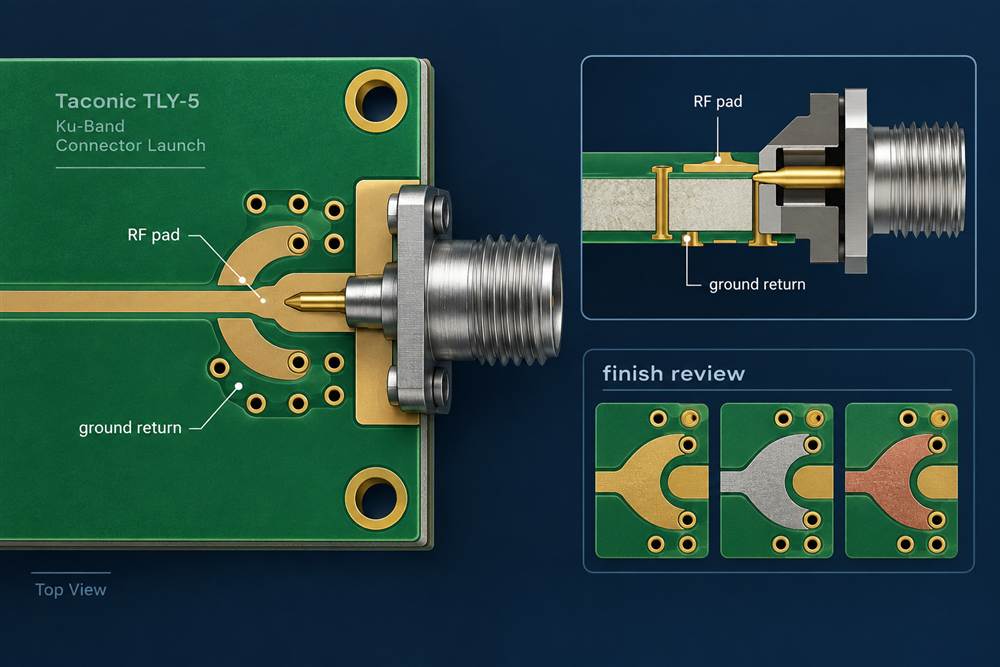
A RF connector launch is most vulnerable where the signal changes environment: connector pin to microstrip, microstrip to embedded stripline, or plated transition to an antenna element. A Taconic TLY-5 PCB launch drawing should show finished pad length, trace neck-down, antipad, ground-via pitch, edge clearance, and the exact reference plane. “50 ohms” alone is not enough to protect phase; the transition needs a geometry that production can inspect and reproduce.
Use controlled-impedance PCB rules for the feed width, but also define the return-via pattern and the keep-out under the connector. A missing return via can force current around a void and add a local inductive section. During design review, compare the electromagnetic model with a dimensioned cross-section and mark every dimension that affects phase. This turns a Taconic TLY-5 PCB simulation assumption into a checkable manufacturing feature.
Common launch risks
- A connector footprint is copied from a lower-frequency design without rechecking pad and antipad scale.
- Mask is opened for solder access but the RF model still assumes bare dielectric.
- Ground stitching is moved during routing to make room for a mechanical datum.
- The array feed is panelized without preserving the same copper balance near each channel.
Control copper, mask, and reference-plane variation
At Ku-band, copper roughness and plated thickness are not cosmetic. A thicker edge or an uneven mask boundary can change the local field distribution; a rougher conductor can increase loss and disturb amplitude balance. The Taconic TLY-5 PCB release should therefore state the copper finish condition, trace-etch expectation, solder-mask treatment, and whether the antenna aperture is mask-free.
When the assembly route requires a PCB assembly step, keep solderable pads separate from the RF aperture. Define the paste opening and the no-clean or cleaning process before the first article. A local mask dam that is acceptable for digital packaging can become an uncontrolled dielectric feature at a Ku-band feed. The right control for a Taconic TLY-5 PCB is not a universal finish; it is a documented interface between the RF model, the board drawing, and the assembly process.
Release a verification package for production
For a first build, release a coupon that follows the same layer pair, copper treatment, and via construction as the antenna feed. The coupon is useful only when its geometry correlates to the product. Record the stackup revision, material lot, pressed thickness, critical trace dimensions, connector seating, and the inspection points that can be repeated on later lots. Do not label a design target as a measured result until the measurement has actually been made.
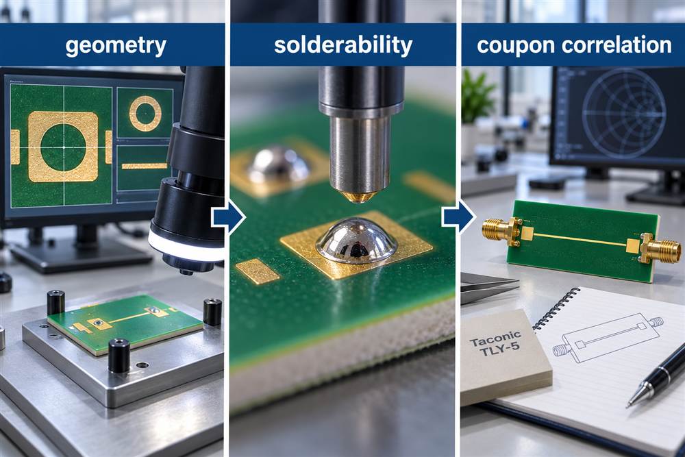
A practical handoff includes the antenna drawing, stackup table, impedance notes, drill and via-fence map, panel orientation, and an engineering-change trigger. If any substitution changes dielectric height, copper profile, finish, or connector interface, route it back through RF review. This is how a Taconic TLY-5 PCB program keeps phase performance stable from prototype to repeat production.
Ku-band release checklist
- Confirm model Dk/Df, pressed thickness, copper, and tolerance assumptions.
- Dimension the connector or antenna launch, including return vias and mask limits.
- Correlate coupon geometry with the product layer pair.
- Define the first-article inspection points and change-control triggers.
- Keep the antenna aperture and assembly process in the same released baseline.
For procurement, a Taconic TLY-5 PCB drawing should carry the same phase-critical dimensions as the released model. Treat a Taconic TLY-5 PCB change as an engineering change whenever the stackup or launch interface moves.
Sources: AGC public TLY-5 material data; Analog Devices RF and mixed-signal layout guidance; Qorvo and RF front-end application practices; KKPCB stackup, fabrication, and RF assembly release methods reviewed for this article.
