
Taconic RF-35 PCB surface finish selection is a launch-interface decision, not a procurement checkbox. A finish changes pad topography, solder wetting, contact behavior, and the geometry the RF current sees at the connector or package transition. The project pain appears when a finish is changed after layout release and the team has no coupon or fixture evidence to separate a pad effect from a stackup effect.
Table of Contents
Define the launch surface before comparing finishes
Start with connector datum, pad length, ground-via fence, solder-mask opening, and the reference plane. Taconic RF-35 PCB geometry must be modeled with the finished copper and pad condition that the supplier can repeat. The RF PCB design design review should state whether the interface is soldered, compression-contact, or probe-based because each one has a different planarity and wear concern.
Balance RF geometry with solderability
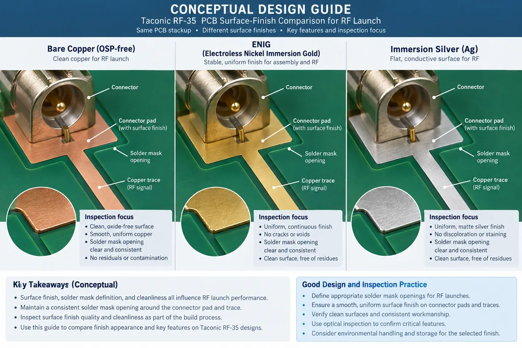
A smooth surface can support a controlled launch, but solderability, storage, exposed copper, and pad robustness still matter. Avoid choosing a finish solely by a typical thickness number. Taconic RF-35 PCB pad and anti-pad dimensions should include finish build-up and etch compensation. The PCB manufacturing manufacturing traveler can then carry thickness target, mask opening, cleanliness, and inspection method together.
Use a finish-matched coupon
A generic impedance strip cannot show a finish-related connector discontinuity. Add a witness with the same pad, mask, via fence, layer pair, and finish as the product. Taconic RF-35 PCB coupon data should be traceable to the same panel. The RF PCB materials controlled-impedance PCB review can compare launch loss, contact condition, and cross-section evidence without confusing a different copper profile with a finish effect.
Protect the launch during assembly
The reflow profile, solder volume, connector coplanarity, and cleaning sequence all influence the finished interface. A board that looks acceptable under optical inspection can still have a different fillet or reference plane. Taconic RF-35 PCB release notes should identify the phase-critical pad. The controlled-impedance PCB assembly record should document inspection and any rework within the launch keep-out.
Release the surface finish with acceptance evidence
Specify typical material values, controlled process targets, and measured acceptance separately. Include pad planarity, solderability, finish thickness, launch dimensions, and RF reference plane in the release review. Taconic RF-35 PCB documentation keeps the material choice traceable, while PCB assembly manufacturing and assembly records show panel, lot, operator, and rework status.
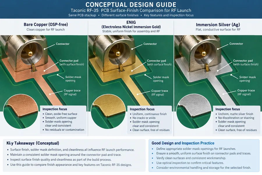
Keep the finish, launch drawing, coupon, and assembly acceptance in one controlled package. That makes the material choice useful to both the RF engineer who needs correlation and the project manager who needs a clear release gate.
Project evidence and handoff for Taconic RF-35 PCB surface finish
For a surface-finish choice, preserve the pad drawing, finish target, mask opening, solderability evidence, launch coupon, connector condition, and assembly profile. A finish change should be reviewed as an RF-interface change, not as a purchasing substitution. The Taconic RF-35 PCB drawing should make the critical datum visible to layout, fabrication, assembly, and test. If a number is calculated, retain the assumptions; if it is a supplier typical, keep it labeled as typical; if it is a measured acceptance value, keep the sample, method, and revision traceable.
| Release item | Engineering question | Evidence to retain |
|---|---|---|
| Stackup and material | Does the finished construction match the RF model? | Finished dielectric target, copper assumption, material lot, cross-section |
| Transition or critical path | Is the mechanical datum also the electrical datum? | Launch drawing, via or pad dimensions, mask and connector inspection |
| Process witness | Does the coupon represent the product feature? | Panel position, layer pair, finish, drill and impedance record |
| Assembly and test | Could placement, rework, or calibration move the result? | Placement tolerance, reflow or rework history, fixture and reference plane |
For program control, use a short disposition statement after each build: what passed, what moved, what is still a target, and which owner decides the next change. This keeps the Taconic RF-35 PCB surface finish discussion focused on evidence and prevents a new material, finish, or layout change from being introduced without an updated model and acceptance plan.
Sources: Taconic and Rogers typical material data; IPC-TM-650 methods relevant to dielectric, copper, drilling, plating, registration, and impedance; RF application guidance from Qorvo, Analog Devices, and Würth Elektronik; KKPCB PCB design, materials, manufacturing, assembly, and high-frequency capability pages. Values are typical, target, or calculated references unless explicitly identified as measured.
