
TLY-5 PCB panelization registration is a project risk when a low-Dk RF design is copied into a manufacturing panel without considering press flow, copper distribution, routing, and assembly tooling. The board may be electrically correct as an individual drawing yet lose connector alignment or channel-to-channel phase consistency after it is nested, laminated, routed, and depanelized.
Table of Contents
Start panelization from RF and mechanical datums
Identify the connector edge, antenna edge, critical via rows, and assembly tooling holes before selecting the array pitch. TLY-5 PCB placement should preserve the same edge reference from artwork through drilling and SMT. The RF PCB design design review can then show whether breakaway tabs, mouse bites, or a routed rail sit inside a keep-out that the RF model assumed was empty.
Balance copper and press construction across the array
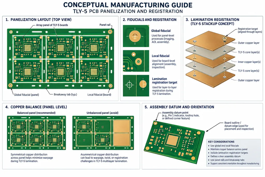
Large copper differences across a panel can change resin flow, local thickness, and registration. Place dummy copper or adjust orientation only when the fabricator can inspect and control it. TLY-5 PCB stackup assumptions should use finished dielectric targets. The PCB manufacturing manufacturing package should document copper balance zones, material construction, press direction, and the cross-section location used for correlation.
Keep coupons and fiducials representative
A coupon at the panel edge may not represent a board in the center. Put impedance, registration, and drill witnesses near the product feature without consuming the assembly fiducial field. TLY-5 PCB coupons should share layer pair and finish with the product. A RF PCB materials high-frequency review can identify which witness is a process monitor and which one is a product-representative acceptance structure.
Plan depanelization before the RF layout is frozen
Router paths, V-score, tabs, support rails, and flexing loads can stress connectors and plated edges. Define the order of routing, inspection, SMT, and final separation. TLY-5 PCB edge clearances must include the actual tool path. The controlled-impedance PCB assembly handoff should specify support, vacuum, connector protection, and any post-depanel inspection near a phase-critical launch.
Close the registration loop with evidence
Use drill-to-copper checks, optical fiducials, cross-sections, and panel maps to show where variation occurred. Do not turn a calculated target into a measured claim. TLY-5 PCB panelization records should carry panel ID, material lot, press cycle, and board position. The PCB assembly manufacturing release can then decide whether to adjust artwork, array orientation, or process—not simply remake the same panel.
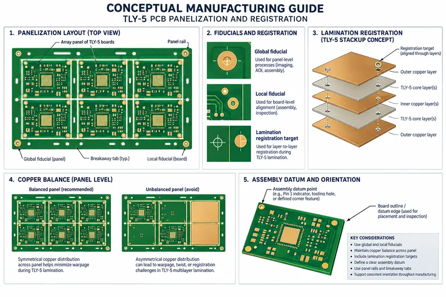
A good panel plan is a controlled experiment: it makes the critical datum visible, puts evidence beside the product, and avoids letting a convenient array shape consume the RF tolerance budget. That approach protects both prototype learning and production yield.
Project evidence and handoff for TLY-5 PCB panelization registration
For a panelized low-Dk board, record panel orientation, board position, press direction, copper map, fiducial map, routed edge, drill witness, and assembly support. The decision is whether the observed shift follows position, process, or artwork. The TLY-5 PCB drawing should make the critical datum visible to layout, fabrication, assembly, and test. If a number is calculated, retain the assumptions; if it is a supplier typical, keep it labeled as typical; if it is a measured acceptance value, keep the sample, method, and revision traceable.
| Release item | Engineering question | Evidence to retain |
|---|---|---|
| Stackup and material | Does the finished construction match the RF model? | Finished dielectric target, copper assumption, material lot, cross-section |
| Transition or critical path | Is the mechanical datum also the electrical datum? | Launch drawing, via or pad dimensions, mask and connector inspection |
| Process witness | Does the coupon represent the product feature? | Panel position, layer pair, finish, drill and impedance record |
| Assembly and test | Could placement, rework, or calibration move the result? | Placement tolerance, reflow or rework history, fixture and reference plane |
For program control, use a short disposition statement after each build: what passed, what moved, what is still a target, and which owner decides the next change. This keeps the TLY-5 PCB panelization registration discussion focused on evidence and prevents a new material, finish, or layout change from being introduced without an updated model and acceptance plan.
Sources: Taconic and Rogers typical material data; IPC-TM-650 methods relevant to dielectric, copper, drilling, plating, registration, and impedance; RF application guidance from Qorvo, Analog Devices, and Würth Elektronik; KKPCB PCB design, materials, manufacturing, assembly, and high-frequency capability pages. Values are typical, target, or calculated references unless explicitly identified as measured.
