
High-frequency board projects often fail at the handoff between an electrical stackup and a buildable panel. A designer may select a low-loss laminate, but the fabricator still needs a controlled dielectric thickness, a stable reference plane, and a practical drill-and-plate sequence. This guide uses an RF-35 PCB design example to show how to convert an RF target into a release package that an engineering and purchasing team can actually review.
RF-35 is a ceramic-filled PTFE/glass material family commonly specified for microwave and RF work. Supplier typical tables list a dielectric constant around 3.50 at 1.9 GHz and a low dissipation factor; these are reference values, not a substitute for the current lot datasheet. The important manufacturing decision is to preserve the intended electromagnetic geometry after lamination, drilling, plating, solder mask, and final routing.
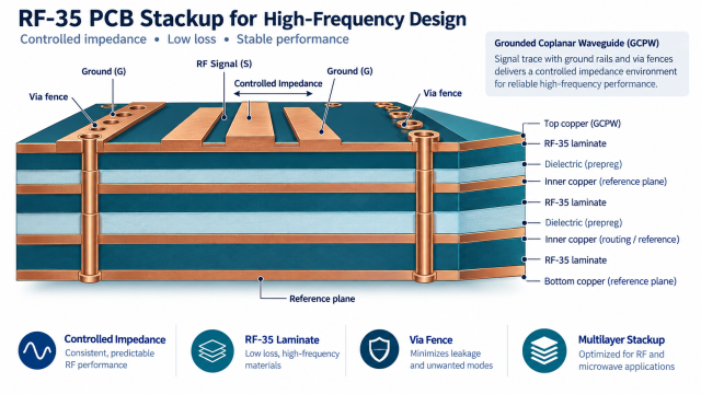
1. Start with the RF-35 PCB stackup, not the trace width
For an RF-35 PCB, impedance is a relationship between copper geometry, dielectric thickness, conductor roughness, and the effective dielectric constant seen by the field. Begin by identifying the signal family: microstrip, grounded coplanar waveguide, stripline, or a transition between them. Then assign a continuous reference plane and define the finished dielectric height after pressing. A nominal core thickness from a catalog is not automatically the finished spacing in a multilayer build.
Define the electrical intent
- State the target impedance and tolerance for each RF net class.
- Identify the frequency band, launch type, connector model, and allowable via stub.
- Show which copper surfaces are reference planes and which are allowed to carry routing.
- Separate RF return paths from noisy digital or power-current paths.
When the board mixes RF and digital functions, a high-frequency PCB review should check field containment, not just line width. A grounded coplanar waveguide may need a via fence and a carefully controlled gap to the side ground. The fence pitch should be treated as an electrical design variable, while the finished drill diameter and registration capability remain manufacturing constraints.
2. Translate material data into a manufacturable impedance model
The RF-35 PCB calculation should use the supplier’s published test method and the fabricator’s stackup coupon plan. Dk values can vary with frequency, resin content, glass style, and the method used to report them. For a first-pass model, document the assumed Dk, copper thickness before and after plating, trace etch compensation, and the pressed dielectric thickness. Record these assumptions in the fabrication drawing so a later material substitution cannot silently change the line impedance.
| Release item | Engineering question | Fabrication response |
|---|---|---|
| Laminate | Which RF-35 grade and thickness are approved? | Confirm available core, prepreg, copper foil, and lot documentation. |
| Trace geometry | What finished width and gap produce the target? | Apply etch compensation and verify minimum features against the panel process. |
| Reference plane | Is the return path continuous through transitions? | Keep voids, antipads, and split planes outside the RF current path. |
| Coupon | How will the build be checked? | Place a representative coupon on the production panel using the same stackup. |
That discipline prevents a common project problem: a simulation that looks correct while the released drawing leaves the fabricator to guess which dielectric thickness or copper state was intended. KKPCB can review the stackup, confirm a suitable process route, and propose a buildable alternative when a requested thickness is not practical.
3. Control transitions, launches, and via fences
On an RF-35 PCB, the connector launch is often the highest-risk section because the field changes from a coaxial structure to a planar one over a short distance. Keep the signal via, ground vias, antipad, and reference-plane clearance in one controlled library footprint. A back-drilled or blind-via option may be justified when a long through stub crosses several layers, but it should be selected from the actual board thickness and drill capability rather than copied from a generic template.
For a grounded coplanar waveguide, place ground vias close enough to maintain the return path while leaving room for drill tolerance and plating. If a via fence is interrupted by a mounting hole, test point, or plane void, document the local return-path exception. This is a more useful review item than simply calling the region “RF keepout.”
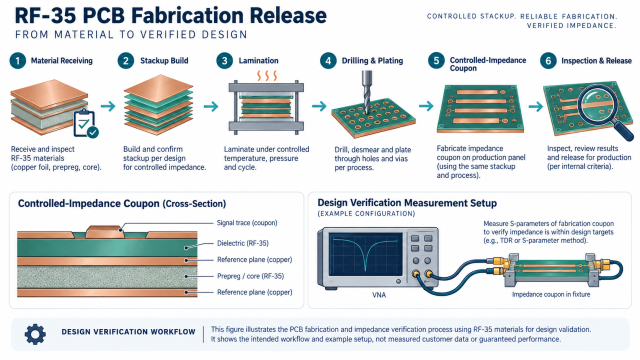
4. Build a production release package
A practical RF-35 PCB release should include the layer stack, impedance table, drill chart, controlled-depth or back-drill notes, copper-finish assumptions, solder-mask restrictions around RF launches, and the coupon location. Add a short DFM checklist covering registration, annular ring, mask dams, thermal relief, and panel orientation. For complex multilayer programs, KKPCB states capability up to 62 layers and 8 sequential lamination steps; the final sequence still needs project-specific confirmation during DFM.
Use the controlled-impedance design review to resolve ambiguous notes before purchasing material. A good review also checks whether the chosen RF PCB materials are compatible with the solder mask, surface finish, thermal cycle, and assembly profile. These decisions are easier to change before tooling than after a panel is released.
Inspection logic
The coupon should represent the critical RF layer pair and use the same copper treatment as the product panel. The final acceptance method may be TDR, a calibrated impedance fixture, or another agreed method. Specify the method and tolerance in the purchase documentation; do not present a design target as a measured result. A multilayer PCB manufacturing partner can then map the requirement to traveler checkpoints for lamination, drilling, plating, and final inspection.
5. Coordinate assembly and bring-up
RF performance can be lost after fabrication if the assembly drawing changes the launch geometry, adds an unplanned solder mask feature, or places a shield fence across the intended return path. Share the RF keepout, connector torque guidance, and rework restrictions with the PCB assembly team. During bring-up, keep the first article configuration traceable: record the approved stackup revision, connector part number, cable launch, and any tuning component value.
In summary, the best RF-35 PCB result comes from a shared definition of material, geometry, transition, coupon, and acceptance method. Treat the stackup as a controlled manufacturing document, not only as an output from a field solver. If the layout, fabrication, and assembly teams review those interfaces together, the design is more likely to reach first-build verification without expensive rework.
Sources: Taconic RF-35 and RF-35P processing guidance and typical property tables; IPC-TM-650 references for dielectric and impedance characterization; and KKPCB manufacturing capability notes. Typical material values are reference data rather than customer measurements, so confirm the current supplier datasheet and lot before release.
