
Table of Contents
A Duroid 6010 PCB impedance coupon is useful only when its geometry, construction, fixture, and acceptance method represent the product feature being released. The project pain point is often a mismatch between the RF model, the coupon panel, and the production board. This guide gives engineers and project managers a disciplined method without inventing measured results or customer case studies.
Why coupon design must follow the RF path
Every Duroid 6010 PCB coupon reflects a finished dielectric-and-copper structure. Press construction, copper foil, etch bias, plating, solder mask, and connector launch geometry affect the evidence. Supplier documentation provides typical material information; the released build needs finished targets, revision control, and a defined process window.
A high-frequency PCB design review should decide which line, via, coplanar gap, or launch is critical before the coupon is drawn. Separate typical material values, design targets, and measured coupon evidence so a process check is not mistaken for product performance.
Seven controls for defensible coupon evidence
1. Match the finished stackup
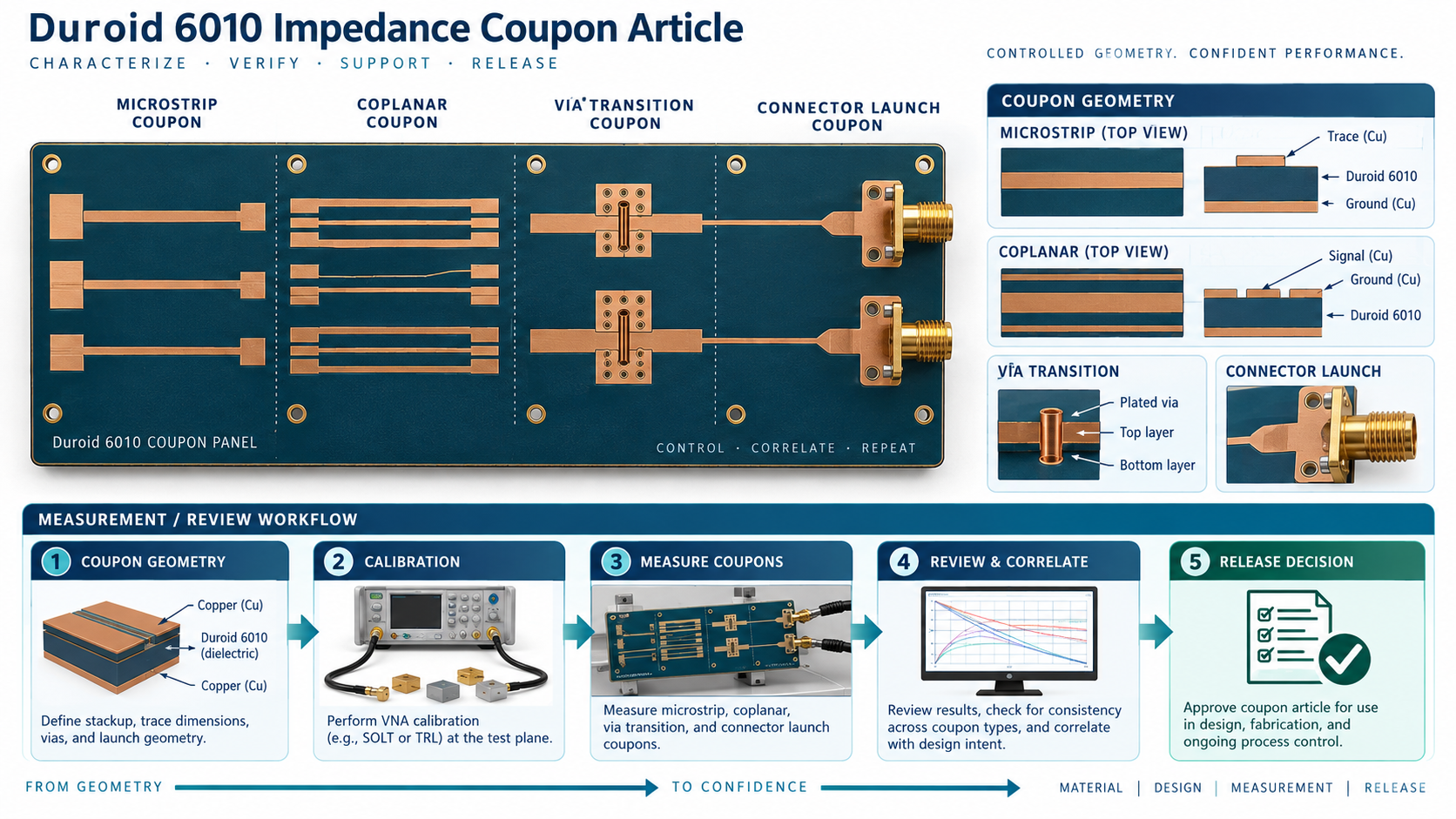
Record post-lamination dielectric targets, copper weights, bondply, press construction, and sequential steps. The coupon stackup must match the product layer pair used by the field model. If the board construction changes, review the coupon before reusing old data.
2. Choose representative geometries
Use microstrip, stripline, grounded coplanar, via-transition, or connector-launch structures as required by the design. Include the line widths, reference-plane distances, mask conditions, and copper assumptions that matter to the product feature.
3. Define the calibration plane
State the fixture, connector interface, calibration method, frequency range, and de-embedding assumptions before measurement. A result without a defined reference plane is difficult to compare across lots or laboratories.
4. Control panel location and traceability
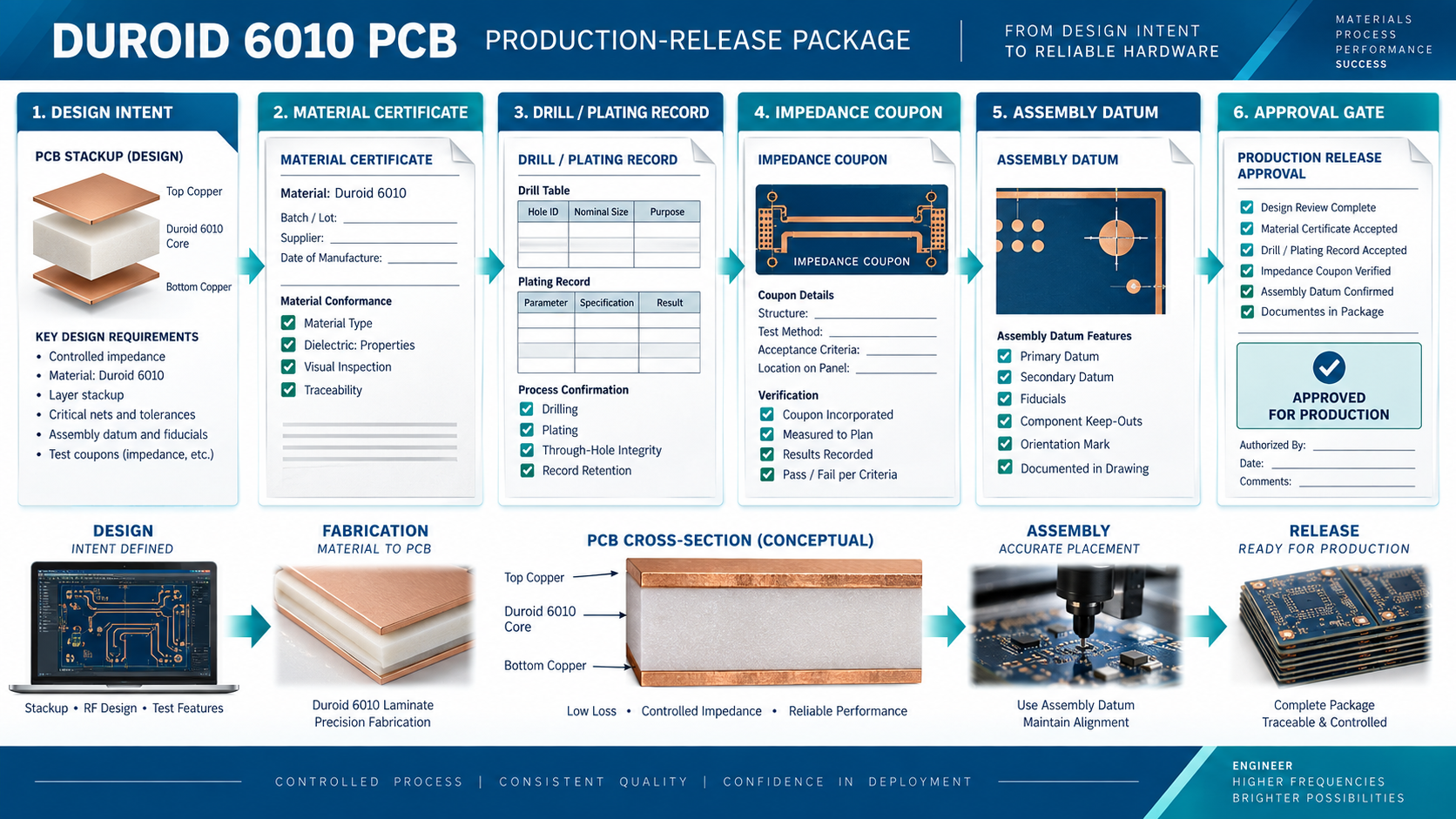
Identify coupon location, panel number, material lot, artwork revision, and fabrication process revision. Keep the coupon map with the panel drawing and inspection record. The PCB manufacturing traveller should record drill, plating, cross-section, and disposition data.
5. Inspect construction before correlation
Use cross-sections and plated-hole checks to confirm that the coupon was built as intended. Check finished dielectric, copper thickness, hole quality, annular rings, mask opening, and registration. Construction evidence comes before correlation to the RF model.
6. Review launch and assembly effects
Connector coplanarity, solder fillets, fixtures, cleaning, and rework can influence the launch. The PCB assembly handoff should retain connector datums, fixture revision, and re-inspection rules. Mark tuning features as engineering options rather than guaranteed results.
7. Tie coupon disposition to release
Define pass/fail criteria, reviewer roles, and escalation paths before the build. If a coupon falls outside the target, identify whether the cause is material, press, copper, drilling, plating, launch, or measurement setup. Do not silently change acceptance limits after seeing a result.
Coupon checklist
- Coupon stackup matches the finished product layer pair.
- Geometry represents the critical line, via, or launch.
- Fixture, calibration plane, frequency range, and method are documented.
- Coupon location, panel, lot, and artwork revision are traceable.
- Cross-section, plated-hole, and registration checks are defined.
- The RF PCB manufacturing review labels typical, target, and measured values separately.
For procurement alignment, the Duroid 6010 PCB material page, the Duroid 6010 PCB fabrication page, and the Duroid 6010 PCB RF capability page should point to one approved coupon and release package. Keep the Duroid 6010 PCB coupon, Duroid 6010 PCB stackup, and Duroid 6010 PCB inspection record under the same revision.
Sources: Rogers Corporation RT/duroid 6010 material information and fabrication guidance; IPC-TM-650 methods for dielectric, drilling, plating, registration, and impedance-related checks; KKPCB internal high-frequency DFM capability notes. Values are typical or target references unless explicitly identified as measured.
