
Table of Contents
A Duroid 6010 PCB can support compact microwave routing, but RF power and thermal design must be released together. The project pain point is the interaction between copper spreading, plated thermal vias, reference-plane continuity, connector mechanics, and environmental conditioning. This guide gives a practical engineering method without claiming unverified customer measurements.
Why thermal and RF paths interact
Every Duroid 6010 PCB is a finished dielectric-and-copper structure. Heat changes dimensions and stresses; copper planes spread heat but can also affect registration and impedance. A material supplier datasheet is a starting reference, while the released board needs finished construction targets and a manufacturable process window.
A high-frequency PCB design review should map hot devices, RF traces, reference planes, thermal vias, board-edge connectors, and keep-outs. Separate typical material values, design targets, and measured coupon evidence.
Seven controls for stable power handling
1. Freeze the finished stackup
Record post-lamination dielectric targets, copper weights, bondply, press construction, and sequential steps. Use the finished cross-section for both thermal and field assumptions. If a proposed substitution changes thickness or copper profile, reopen the impedance and heat-path review.
2. Define the heat path
Show component pads, thermal vias, copper spreaders, and reference planes on one cross-section. Thermal vias should connect to the intended plane without creating an uncontrolled RF void. Specify via, pad, and keep-out strategy so thermal and RF teams do not optimize different layers.
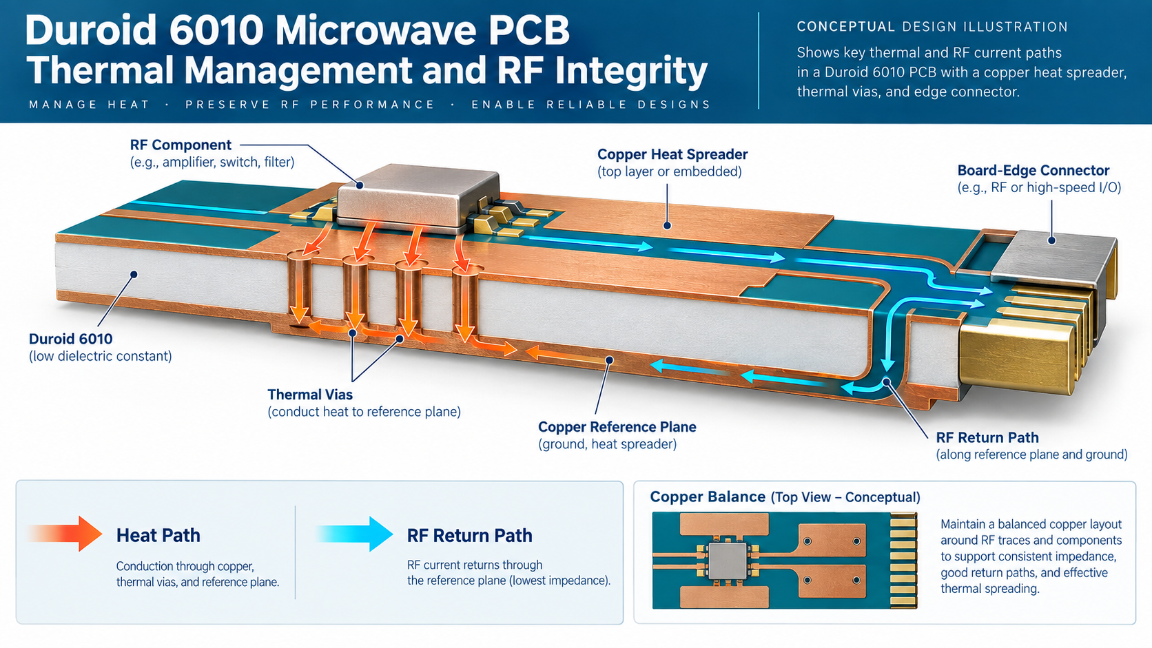
3. Balance copper and panel stress
Large copper areas, thermal planes, and RF voids influence lamination and etch balance. Use a balanced panel map, tooling plan, and fiducial strategy. The PCB manufacturing traveller should tie copper balance, etch compensation, registration, and cross-section locations to one revision.
4. Protect RF return continuity
Keep reference planes continuous around thermal-via fields and connector launches. Place ground stitching where the field model requires a short return path. If a heat spreader forces a plane opening, include that opening in the RF review instead of treating it as a mechanical-only feature.
5. Carry datums into assembly
Connector seating, solder fillets, fixtures, and board support can move a launch. The PCB assembly traveler should retain connector datums, mask openings, and the approved stackup revision. Identify rework rules and re-inspection points before release.
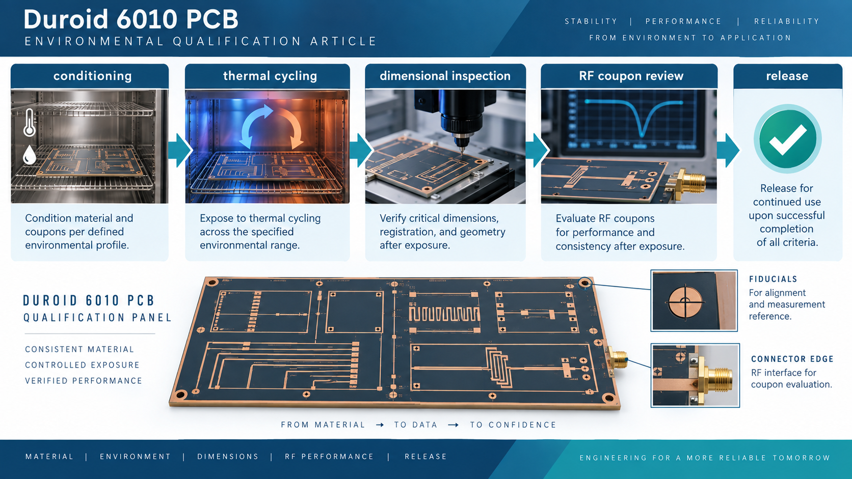
6. Separate conditioning from qualification
Define how material and fabricated coupons are conditioned before environmental or RF evaluation. The sequence, dwell, and inspection method must be agreed before the build; otherwise teams may compare different states of the same lot.
7. Use representative coupons
Choose coupons representing the critical line, via, or connector transition. Define coupon location, fixture, calibration, frequency range, and acceptance method before panel release. Coupon evidence belongs to that controlled revision and is not a customer case study.
Engineering checklist
- Finished dielectric, copper, drill, and thermal-via targets are revision controlled.
- RF and thermal assumptions use the same cross-section and reference planes.
- Panel copper balance, fiducials, and registration checks are defined.
- Connector datums and assembly fixtures match the fabrication drawing.
- Conditioning, coupon, and acceptance methods are written before production.
- The RF PCB manufacturing review labels typical, target, and measured values separately.
For procurement alignment, the Duroid 6010 PCB material page, the Duroid 6010 PCB fabrication page, and the Duroid 6010 PCB RF capability page should point to the approved construction. Keep the Duroid 6010 PCB thermal map, Duroid 6010 PCB stackup, and Duroid 6010 PCB inspection record under one revision.
Sources: Rogers Corporation RT/duroid 6010 material information and fabrication guidance; IPC-TM-650 methods for thermal, drilling, plating, registration, and impedance-related checks; KKPCB internal high-frequency DFM capability notes. Values are typical or target references unless explicitly identified as measured.
