
Table of Contents
A Duroid 6010 PCB can be electrically well designed and still miss the project’s RF margin when layer-to-layer registration, copper balance, or board-edge datums drift through lamination and etch. The real engineering challenge is coordinating material behavior, panel process, and inspection evidence before the build is released. This guide provides a practical method for engineers and project managers without presenting unverified customer measurements.
Why dimensional drift affects RF builds
Every Duroid 6010 PCB is a finished stack of dielectric and copper. Press construction, copper distribution, tooling, drilling, and etch compensation influence feature placement and the distance to a reference plane. Supplier documentation describes material behavior, but the released construction must define finished targets and a process window.
A high-frequency PCB design review should identify critical RF features, fiducials, connector datums, tooling holes, and edge clearances. Keep typical material values, design targets, and measured inspection results separate. If a panel or press proposal changes, update the stackup and registration review together.
Seven controls for registration stability
1. Balance copper before panelization
Map large copper pours, RF lines, thermal planes, and voids on every layer. Balanced copper reduces process asymmetry and makes etch compensation more predictable. The PCB manufacturing traveller should connect copper balance, panel map, tooling, and cross-section locations to one revision.
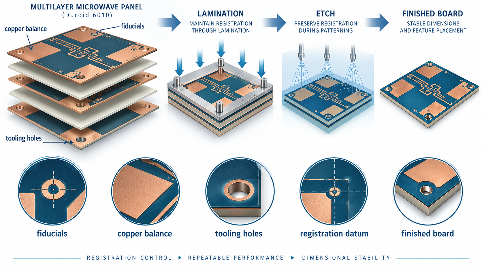
2. Establish a registration datum chain
Use stable tooling holes and fiducials to relate artwork, drill, lamination, and routing. Mark which datum controls each RF connector, via field, and board edge. Do not rely on a single local mark when the critical features span several layers.
3. Define finished dielectric targets
Record post-lamination thickness for each RF layer pair and include bondply and sequential steps. The electrical model should use the finished construction, not only nominal catalogue values. If the finished dielectric changes, reopen trace width, via, and impedance assumptions.
4. Tie etch compensation to line intent
State intended line width, copper thickness, mask opening, and compensation approach. Keep test patterns or coupons representative of the critical lines. Changes in copper profile or plating can move effective impedance even when artwork coordinates are unchanged.
5. Protect via and connector registration
Specify finished holes, annular rings, antipads, via fences, and connector pads as registration-critical features. A multilayer PCB release should identify sequential-lamination and back-drill constraints alongside the RF drawing. Carry the same edge datum into the assembly fixture.
6. Inspect cross-section and plated holes
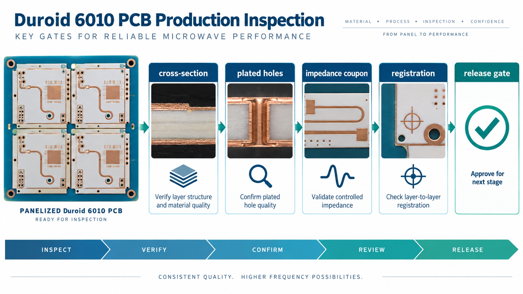
Define where cross-sections are taken, what holes are representative, and how plating and registration are dispositioned. A cross-section confirms the construction used for the lot; it does not replace a complete product test. Record lot, panel, and coupon identifiers.
7. Use a staged release gate
Move from material verification to finished-dielectric review, etch compensation, drilling/plating, coupon review, and final registration acceptance. The RF PCB manufacturing review should label each result as typical, target, or measured and state which release decision it supports.
Project checklist
- Panel copper balance, tooling holes, fiducials, and datums are revision controlled.
- Finished dielectric targets match the field model and fabrication drawing.
- Etch, plating, and mask assumptions are documented for critical RF lines.
- Via, connector, and board-edge registration limits are manufacturable.
- Cross-section, coupon, and inspection locations are defined before production.
- Material lot, panel map, and disposition remain traceable to the release.
For procurement alignment, the Duroid 6010 PCB material page, the Duroid 6010 PCB fabrication page, and the Duroid 6010 PCB RF capability page should point to one approved construction. Keep the Duroid 6010 PCB drawing, Duroid 6010 PCB panel map, and Duroid 6010 PCB inspection record under the same revision.
Sources: Rogers Corporation RT/duroid 6010 material information and fabrication guidance; IPC-TM-650 methods for dielectric, drilling, plating, registration, and impedance-related checks; KKPCB internal high-frequency DFM capability notes. Values are typical or target references unless explicitly identified as measured.
