
Contents
Duroid 5880 PCB connector launches are a common project pain point. A layout can meet the simulated impedance target and still show return-loss variation when the connector datum, plated holes, solder fillet, or ground-via pattern changes during assembly. This guide gives an engineering handoff for repeatable RF launch fabrication without claiming customer measurements.
Why the connector launch controls RF yield
An edge launch is a short transmission-line transition that combines the connector, signal pad, reference plane, ground pads, mounting holes, and the first return vias. On a Duroid 5880 PCB, the transition is sensitive to the finished dielectric, copper thickness, pad geometry, and mechanical seating. Treat the launch as one RF and mechanical structure rather than a footprint copied between projects.
Freeze the approved Duroid 5880 PCB drawing, connector part number, stackup, and panel datum together. A high-frequency PCB design review should show the launch cross-section, return-current path, and keep-outs at the same revision.
Layout and datum controls
1. Establish a connector datum
Every Duroid 5880 PCB launch should reference this datum through panel, drill, and assembly documentation.
Dimension the connector mounting holes, signal pad, ground pads, and first via row from one mechanical datum. Do not reference a routed board edge that may move after profiling. The datum should also appear on the panel drawing, fixture drawing, and assembly traveler.
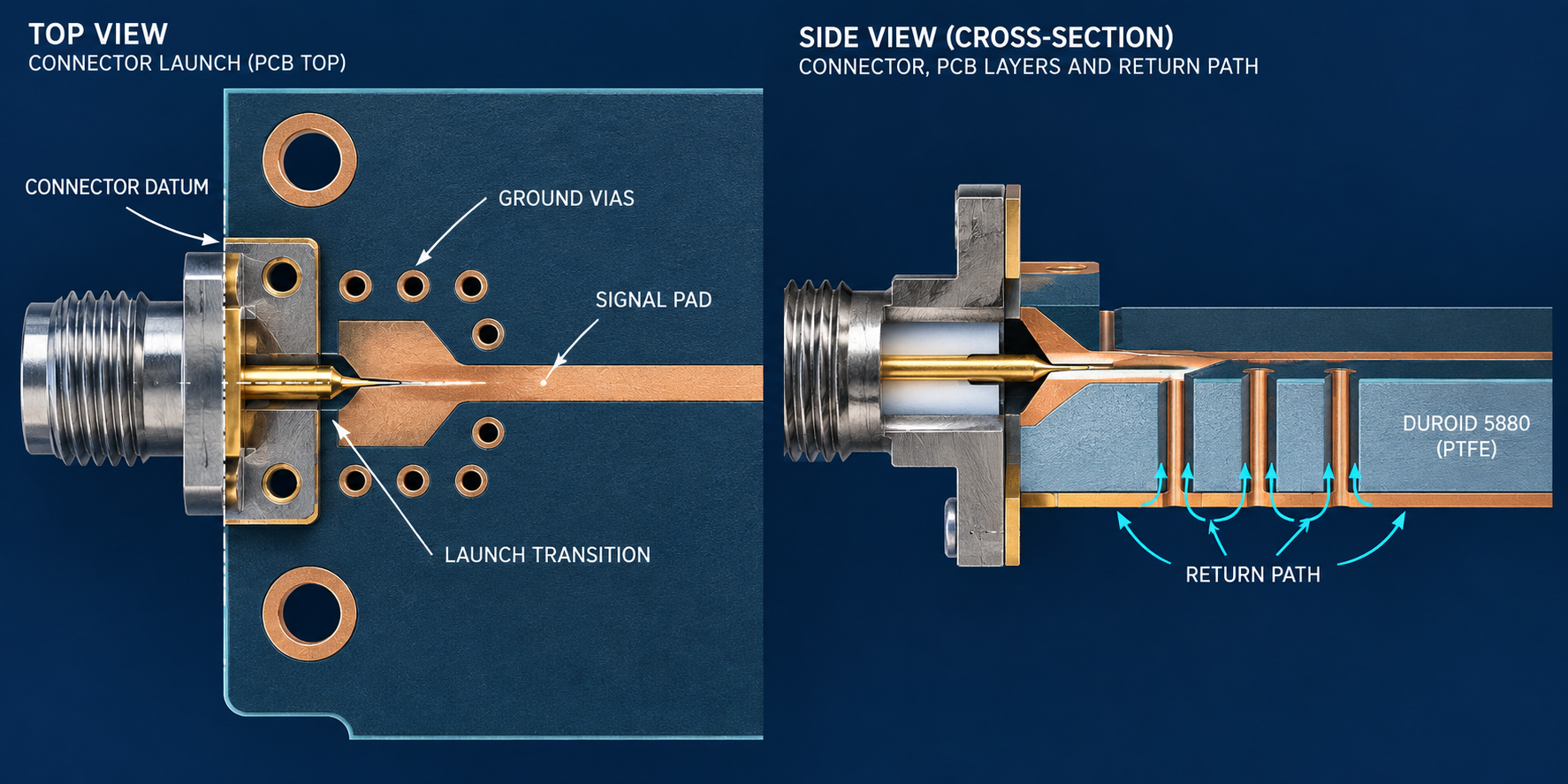
Conceptual connector-launch datum, signal pad, ground vias, and return path.
2. Control the transition geometry
On a Duroid 5880 PCB, a small launch change can alter the return-current path.
Keep the launch trace, pad taper, ground clearances, and via fence tied to the approved field model. When the connector supplier changes, compare pin diameter, flange, mounting hardware, and insertion depth before releasing the new footprint. Material data from a laminate supplier is not a finished-board impedance guarantee.
3. Lock stackup and finished dielectric targets
The approved Duroid 5880 PCB material package should identify the construction revision.
Record the press construction, copper foil, finished dielectric target, and any sequential-lamination steps in the PCB materials package. If a Duroid 5880 PCB uses a different core or bondply, rerun the launch field review instead of copying the prior trace width.
4. Give the return current a nearby path
A Duroid 5880 PCB drill and plating review must preserve the intended return path.
Ground vias around the connector should connect to the intended reference plane with a geometry that fits the drill and plating process. Avoid a via-fence break at the launch unless the field model and fabrication drawing both show it. A PCB manufacturing review should confirm finished hole, annular ring, registration, and copper balance.
Assembly and inspection controls
5. Control seating and solder
The Duroid 5880 PCB connector must remain seated against the approved mechanical reference.
Define how the connector is seated, supported, soldered, and cleaned. A solder fillet that pulls the connector off datum can change the launch more than a small trace-width adjustment. The PCB assembly traveler should identify the fixture, solder process, torque sequence, and visual or X-ray inspection points.
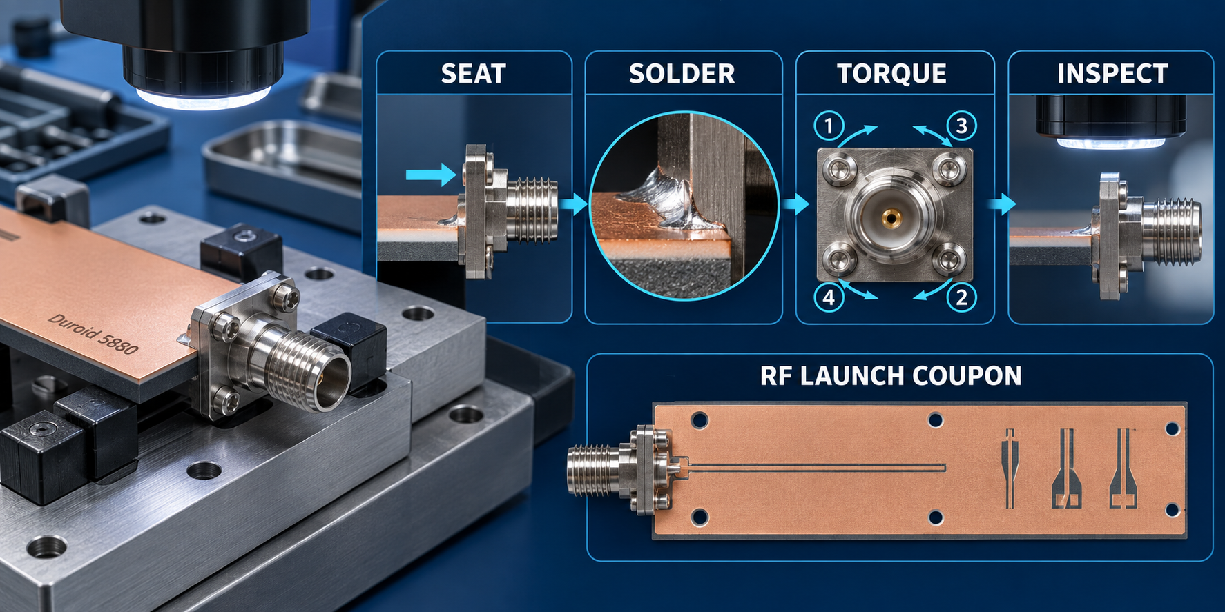
Conceptual seat, solder, torque, inspection, and RF launch coupon flow.
6. Use a representative launch coupon
When electrical correlation is required, place a representative launch coupon on the panel and define the fixture, calibration, frequency range, and acceptance method before production. The coupon demonstrates process evidence for that revision. It is not a customer result, and it should not be presented as one.
7. Inspect center and edge locations
For a Duroid 5880 PCB panel, retain center and edge evidence with the same revision.
For each Duroid 5880 PCB panel, retain center and edge evidence with the same revision.
Panel density, copper fill, and routing can create different registration conditions at the center and edge. Inspect the connector datum, plated holes, and launch pads at representative locations. Retain the inspection map with the multilayer PCB build record.
Duroid 5880 PCB connector-launch release checklist
- Connector, pad, holes, and return vias share one datum.
- Approved stackup and finished dielectric targets are revision controlled.
- Signal and ground geometry are checked against the field model.
- Drill, plating, annular-ring, and registration limits are manufacturable.
- Seating, solder, torque, cleaning, and inspection steps are documented.
- A launch coupon is labeled as process evidence, target, or measured data.
The approved Duroid 5880 PCB launch should remain synchronized across design, fabrication, and assembly. KKPCB can review the stackup, connector footprint, datum scheme, via geometry, and inspection plan as a single release package.
Sources: Rogers Corporation RT/duroid 5880 material information and fabrication guidance; IPC-TM-650 methods for drilling, plating, registration, and solder inspection; KKPCB internal high-frequency DFM capability notes. Values are typical or target references unless explicitly identified as measured.
