
Contents
Duroid 5880 PCB projects for outdoor radar often fail at the mechanical-to-RF interface rather than in the laminate specification. Seasonal temperature, moisture conditioning, panel handling, and connector datum changes can move a launch or array cell enough to change phase balance. This engineering guide gives a production review method for dimensional stability and registration without presenting unverified customer measurements.
Duroid 5880 PCB dimensional stability and RF registration
RT/duroid 5880 is a low-loss PTFE composite, but the finished board is still a laminated structure with copper, drilled holes, plated barrels, solder mask, and mechanical datums. Each process step can add a small shift. For a radar panel, the important question is not whether one coupon looks flat. The question is whether the antenna geometry, reference planes, holes, and connector launch remain registered after the planned process sequence.
Start the design review with the Duroid 5880 PCB drawing, approved stackup, material lot, copper weights, drill table, and panel map. Mark the origin used by layout, fabrication, assembly, and inspection. A high-frequency PCB design review should use that same origin when it checks array pitch, feed length, and reference-plane continuity.
Seven Duroid 5880 PCB controls that keep registration predictable
1. Freeze the panel datum
Every Duroid 5880 PCB panel should use this datum as the reference for all downstream checks.
Define a master datum before array replication. Put tooling holes and optical fiducials outside the active RF keep-out, then dimension antenna cells and connector features from the datum rather than from a routed edge. This prevents a trimmed edge or a shifted outline from becoming an unintended reference.
2. Separate material data from the stackup target
Manufacturer data is a starting point for dielectric constant, dissipation factor, and thickness. It is not a promise that every pressed construction will have the same effective impedance. Record the approved press cycle, copper foil, resin content, and finished dielectric target in the PCB materials package. If a core or bondply changes, rerun the controlled-impedance review.
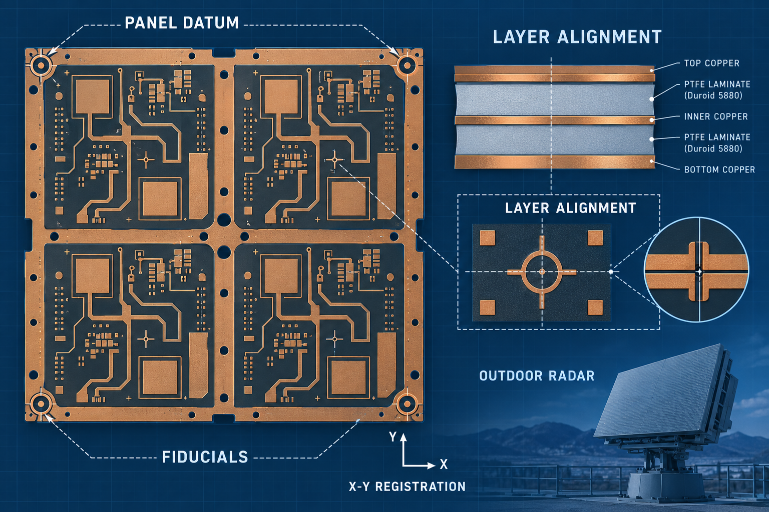
Conceptual panel datum, fiducials, and layer-alignment targets for an outdoor radar panel.
3. Use fiducials that survive fabrication
On a Duroid 5880 PCB, fiducials must remain readable after imaging, drilling, and surface finish.
Place global fiducials where the fabricator can image them consistently and local fiducials where the assembly machine needs them. Keep copper, mask, and silkscreen clearances explicit. The inspection plan should compare the same fiducial pair before and after imaging, drilling, and surface finish.
4. Control drill and copper registration together
A production release should keep a second Duroid 5880 PCB panel reference for drill compensation and edge-to-center comparison.
A hole can be in tolerance relative to its drill program and still be wrong relative to the RF pad. Review drill compensation, annular ring, layer-to-layer registration, and panel stretch as one chain. A PCB manufacturing handoff should show the drill origin, compensation revision, tooling scheme, and cross-section locations.
5. Protect the connector datum
The Duroid 5880 PCB connector launch should never inherit an untracked edge reference.
Connector mounting holes, launch pads, and the first return vias should share the mechanical datum used by the RF drawing. When a connector vendor changes, compare the new footprint and insertion depth against that datum. The PCB assembly traveler should call out seating, solder, torque, and inspection features that can move the launch.
6. Plan environmental conditioning without inventing results
The Duroid 5880 PCB RF drawing and the conditioning plan should share the same registration datum.
For an outdoor project, define the conditioning sequence, dwell points, recovery time, and inspection method before release. Use a representative coupon or witness panel to check whether the registration target remains readable after the agreed cycle. Report the result as a target, typical value, or measured value; never label a conceptual check as a customer qualification.
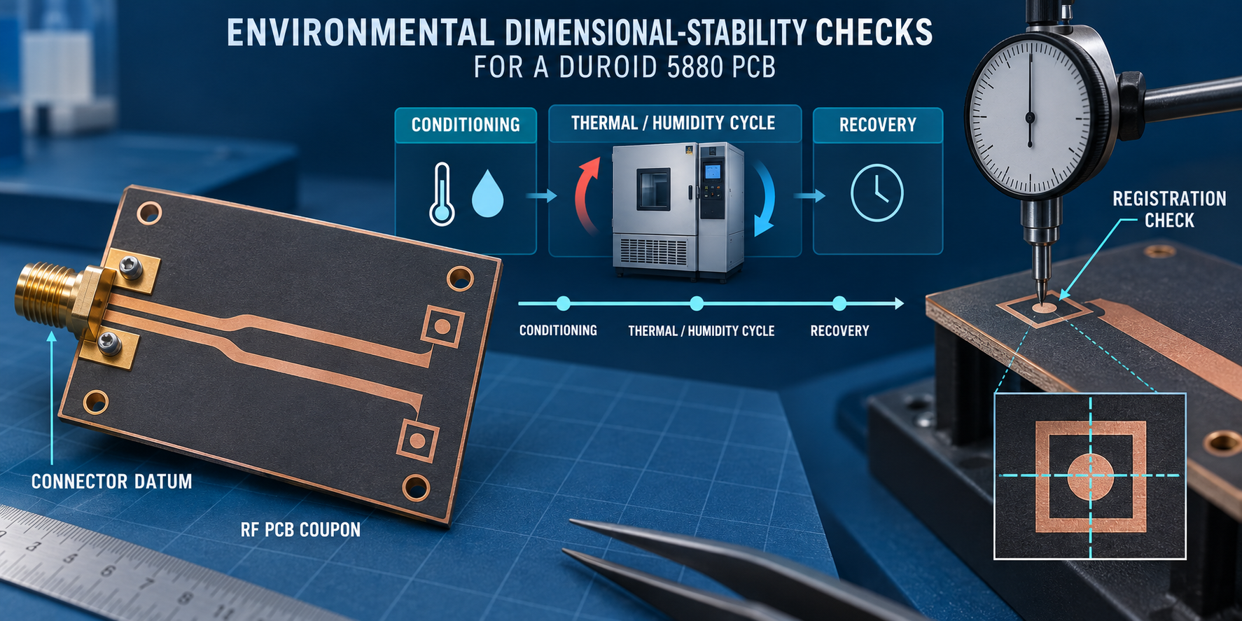
Conceptual conditioning, recovery, connector datum, and registration inspection sequence.
7. Close the loop in panel and assembly review
For a Duroid 5880 PCB release, retain the panel map with the assembly traveler.
Review center and edge locations when copper density is uneven. Confirm that the same panel revision reaches drilling, lamination, imaging, routing, and assembly. If the board is part of a multilayer PCB build, check sequential-lamination datums and any back-drilled features. Retain the inspection map with the manufacturing traveler.
Practical release checklist for an outdoor radar build
For each Duroid 5880 PCB release, compare the same datum, fiducials, and connector reference. A second Duroid 5880 PCB lot should follow the identical inspection map before engineering approval.
- One origin is shared by layout, panel, drill, assembly, and inspection.
- Stackup, material lot, copper, and finished dielectric targets are version controlled.
- Global and local fiducials have clear copper, mask, and silkscreen rules.
- Connector holes, launch pads, and return vias reference one mechanical datum.
- Registration checks distinguish engineering targets from measured evidence.
- Center and edge samples are retained when panel density or copper fill changes.
The approved Duroid 5880 PCB stackup should also stay synchronized with panel and assembly revisions.
KKPCB can review a Duroid 5880 PCB data package for stackup, fiducials, registration, drilling, and assembly handoff. The objective is a board that keeps its RF geometry aligned through fabrication and outdoor qualification planning, not a claim of a specific field result.
Key takeaway for Duroid 5880 PCB programs
Dimensional stability is a system control. A fixed datum, controlled stackup, survivable fiducials, coordinated drill compensation, and a documented conditioning plan give every Duroid 5880 PCB project a repeatable path from RF layout to production release.
Sources: Rogers Corporation RT/duroid 5880 material information and fabrication guidance; IPC-TM-650 methods for dimensional, drilling, plating, and registration checks; KKPCB internal high-frequency DFM capability notes. Values are typical or target references unless explicitly identified as measured.
