
At 5G frequencies, an artwork line that looks correct on screen can leave the factory with a different width, edge shape, or solder-mask clearance. The change is usually small, but the same change repeated across an antenna feed can move impedance and phase. This guide shows how an RO4003C PCB release can use etch compensation and mask rules to protect RF intent without inventing unverified production results.
Why RF line dimensions move during fabrication
Outer-layer copper is affected by foil profile, imaging bias, etch rate, plating build, and the distance to nearby copper. Solder mask adds another variable because the opening can shift relative to a fine trace or pad. For a high-frequency PCB, the RO4003C PCB drawing should identify which dimensions are finished requirements and which are artwork targets. That distinction lets the process engineer choose compensation without changing the electrical goal.

Define the electrical reference before compensation
Start with the finished copper assumption, dielectric thickness, reference-plane location, and the impedance target. Rogers data lists typical RO4003C material values, but the design value is not a substitute for the finished stackup supplied by the fabricator. On a new RO4003C PCB, release a controlled-impedance table that connects line width, spacing, copper thickness, and the test coupon to one stackup revision.
RO4003C PCB artwork targets versus finished requirements
Every RO4003C PCB drawing should show the finished feature and the process allowance as separate, reviewable items.
Use a two-column drawing note: one column for the finished feature that the RF model needs, and one for the artwork or process allowance used to reach it. This keeps etch compensation from being mistaken for a wider electrical trace. It also gives inspection a clear question: is the measured feature inside the finished requirement, and was the artwork revision the one approved for this lot?
| Feature | Typical risk | Release question |
|---|---|---|
| RF trace width | Etch bias changes impedance | Is the finished width defined at the correct copper surface? |
| Trace-to-plane spacing | Uneven copper density shifts the edge | Does the stackup drawing show the actual reference plane? |
| Mask opening | Registration or web can load the feed | Is the mask keep-out checked against the RF field? |
| Launch pad | Plating and corner rounding change the transition | Are pad, mask, and drill datums tied to one origin? |
Keep solder mask away from sensitive fields
Mask is not automatically electrically neutral at an RF launch. A mask web that narrows a gap or bridges a pad can change the local capacitance and create unit-to-unit variation. Treat the mask opening as a designed feature, especially around an edge connector, antenna feed, or exposed transition. If the build uses controlled impedance PCB rules, include mask-clearance assumptions in the review instead of checking them only after Gerber output.
Use coupons that represent the real line
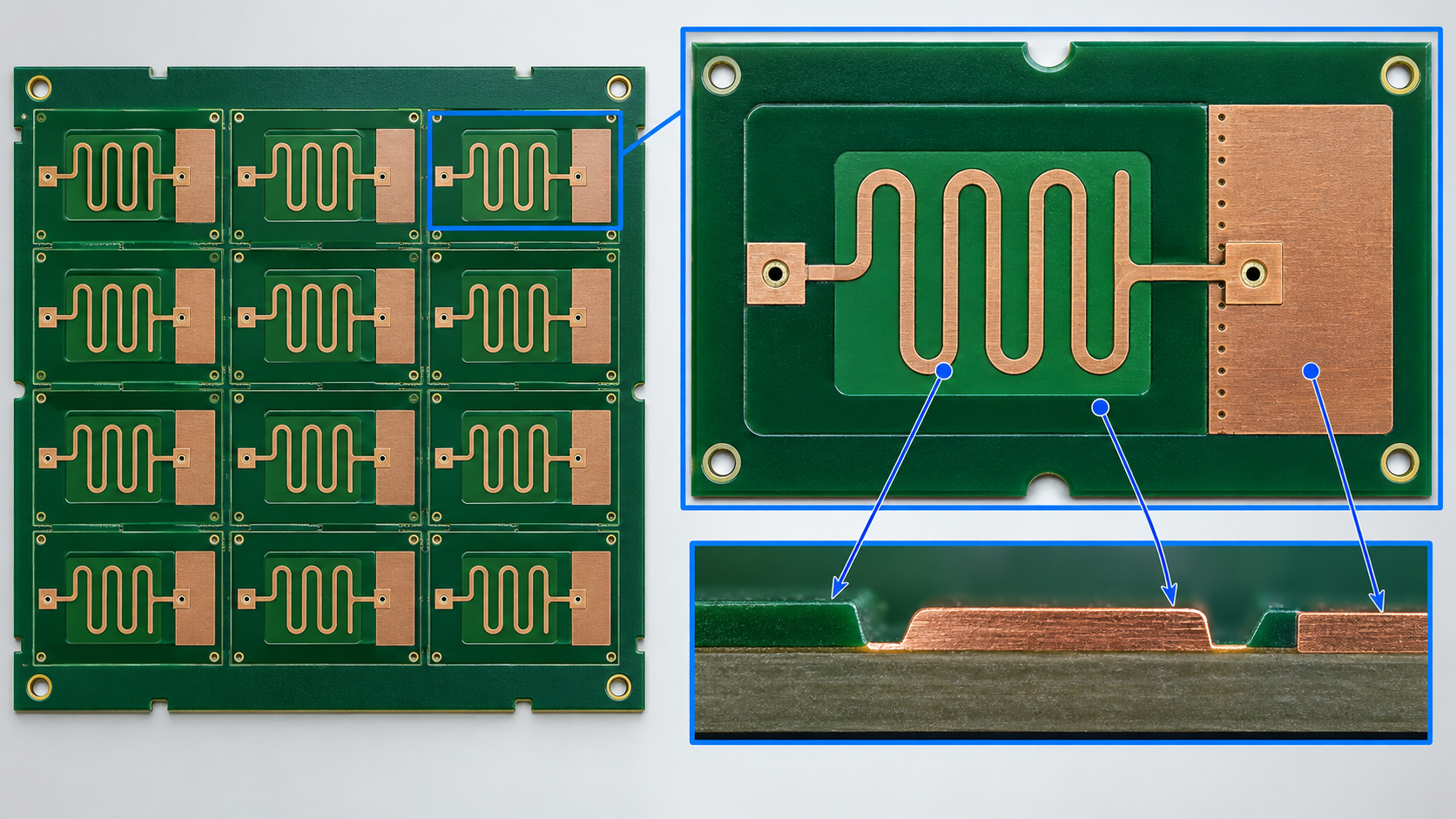
An etch coupon should use the same copper layer, plane relationship, line style, and surface-finish route as the sensitive RF feature. A generic wide trace can prove that copper exists, but an RO4003C PCB coupon must preserve but it cannot explain a narrow feed transition. Place the coupon where panel copper density and orientation are representative. The coupon is a process witness, not a customer measurement, so the release should say what it can and cannot prove.
Correlate inspection to the approved artwork
Record artwork revision, panel ID, copper weight, and finish with each coupon review. Compare line width at more than one panel position when the panel has a strong copper-density gradient. If the result moves with panel position, review copper balance and imaging registration before changing the RF geometry. If the result moves with finish or plating route, keep the electrical target fixed and review the process allowance.
DFM checks before releasing an RO4003C PCB
- Mark finished RF dimensions separately from artwork compensation.
- Show mask openings and keep-outs around feeds, launches, and antenna apertures.
- Confirm the approved stackup, copper weight, and surface-finish route.
- Use a coupon that matches the RF layer pair and line style.
- Review copper balance without placing fill in an RF keep-out.
- Link every drawing revision to the panel and inspection record.
KKPCB can review an RF PCB manufacturing package for artwork bias, mask registration, coupon coverage, and drawing clarity. A practical review separates target values, typical laminate data, and measured values so the project team knows what still needs validation.
Key takeaway
Reliable RO4003C PCB fabrication begins when the electrical target is separated from the process allowance. A clear RF drawing, a representative coupon, and a mask-aware inspection plan keep etch compensation from becoming a hidden design change. The same RO4003C PCB production logic scales from a single antenna feed to a production panel: define the finished requirement, document the route to it, and preserve traceability.
Sources: Rogers Corporation RO4000 series laminate data sheet and RO4003C product information; IPC-TM-650 dimensional, solder-mask, and impedance test methods; KKPCB internal DFM capability notes. Any material figures are typical references, not customer measured results.
