What is a Fine Line PCB?
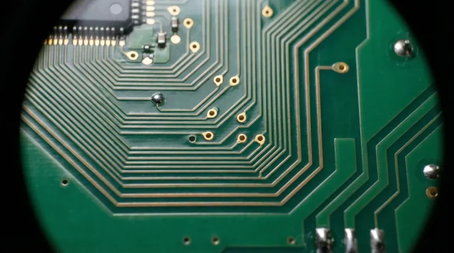
A Fine Line PCB refers to a printed circuit board with extremely narrow trace width and spacing, typically below 100 μm (4 mil) and often reaching 50 μm (2 mil) or less in advanced designs.
These PCBs are essential for high-density interconnect (HDI) and miniaturized electronic products, where space is limited and circuit complexity is high.
Why Fine Line PCB Matters
As electronic devices become smaller and more powerful, PCB designs must:
- Fit more components in limited space
- Support higher signal density
- Maintain signal integrity at high speed
Typical Fine Line Capabilities
| Capability Level | Line Width / Spacing |
|---|---|
| Standard PCB | ≥ 100 μm (4 mil) |
| Fine Line PCB | 50–100 μm (2–4 mil) |
| Advanced HDI | 25–50 μm (1–2 mil) |
| IC Substrate Level | < 25 μm |
Key Technologies Behind Fine Line PCB
1. HDI (High-Density Interconnect)
- Uses microvias and multiple build-up layers
- Enables compact and complex routing
2. Laser Drilling
- Required for precise microvia formation
- Essential for multilayer fine pitch designs
3. Advanced Imaging (LDI)
- Laser Direct Imaging ensures accurate trace definition
- Reduces misalignment issues
4. Semi-Additive Process (SAP / mSAP)
- Enables ultra-fine traces with better precision
- Common in high-end PCB and substrate manufacturing
Materials for Fine Line PCB
Material stability is critical for fine line accuracy:
- FR4 (High Tg) → standard HDI
- BT Epoxy → IC substrate and packaging
- ABF (Ajinomoto Build-up Film) → ultra-fine semiconductor substrates
Applications of Fine Line PCB
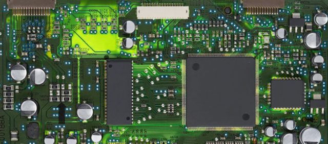
1. Smartphones & Wearables
Compact designs require high-density routing.
2. IC Substrates
Fine lines are essential for chip interconnection.
3. High-Speed Computing
Servers and processors require dense signal routing.
4. Automotive Electronics
ADAS and control modules need compact, reliable PCBs.
5. Medical Devices
Miniaturization is critical for portable equipment.
Manufacturing Challenges
Fine Line PCB is one of the most difficult PCB types to produce:
1. Etching Precision
Over-etching or undercut can destroy fine traces.
2. Registration Accuracy
Layer alignment must be extremely precise.
3. Yield Control
Smaller features = higher defect risk.
4. Cleanroom Requirements
Dust or contamination can cause open/short circuits.
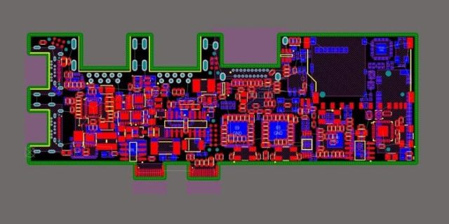
Design Considerations
1. Avoid Overly Aggressive Line Width
Design within manufacturable limits.
2. Control Stack-up Carefully
Layer structure impacts impedance and manufacturability.
3. Consider Signal Integrity
Fine lines often carry high-speed signals.
4. Work Closely with Manufacturer
DFM (Design for Manufacturability) is critical.
When Do You Need a Fine Line PCB?
Choose Fine Line PCB when:
- Your design is highly compact
- You require high pin-count components
- HDI or microvia structures are needed
- Signal density is very high
Avoid it if:
- Standard PCB can meet requirements
- Cost is the primary concern
- Design complexity is low
Conclusion
Fine Line PCB technology enables the development of compact, high-performance, and high-density electronic products. However, it requires advanced manufacturing capabilities and strict process control.
Choosing the right PCB manufacturer is critical to ensure precision, yield, and reliability.
