What Is a Logic Test PCB?
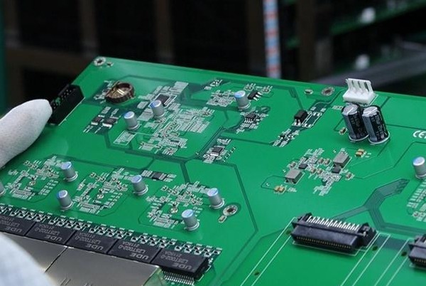
A Logic Test PCB is a specialized digital test PCB used to verify the functionality, timing, and performance of digital ICs and high-speed logic devices.
Unlike standard circuit boards, a Logic Test PCB is designed as part of an ATE PCB system, where accurate signal delivery and measurement are critical.
Typical use cases include:
- Digital IC validation
- FPGA and processor testing
- Memory interface verification
- High-speed logic system debugging
A Logic Test PCB is not just a test board—it is a precision platform for digital signal validation.
Why Logic Test PCB Design Is Critical
In high-speed digital systems, even small signal issues can cause incorrect test results. A poorly designed Logic Test PCB can lead to:
- Timing errors and skew
- Signal reflection and ringing
- Crosstalk between channels
- Data corruption during testing
These problems directly affect test accuracy, yield, and product reliability.
Key principle:
In a Logic Test PCB, signal integrity determines test credibility.
Core Architecture of a Logic Test PCB
A well-designed Logic Test PCB includes several key functional blocks:
- High-Speed Signal Routing Region
Handles digital signals such as DDR, PCIe, and SerDes - Power Distribution Network (PDN)
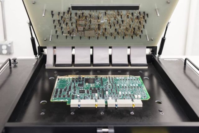
Provides stable voltage for DUT and test circuits - Test Socket Interface
Connects the DUT with consistent mechanical and electrical contact - ATE Interface Connectors
Enable communication between the test system and the PCB - Grounding & Shielding Structure
Reduces noise and ensures signal return paths
Each block must be optimized to ensure accurate and repeatable digital testing.
Signal Integrity in Logic Test PCB Design
Signal Integrity (SI) is the most critical factor in Logic Test PCB performance:
- Controlled Impedance Routing
Maintain consistent impedance for all high-speed signals - Length Matching
Critical for timing-sensitive interfaces like DDR - Minimized Crosstalk
Proper spacing and ground shielding between traces - Clean Return Paths
Continuous ground planes reduce noise - Via Optimization
Reduce via stubs and signal discontinuities
At high speeds, the Logic Test PCB itself becomes part of the signal path.
Timing & Synchronization Challenges
Logic Test PCBs must ensure precise timing alignment:
- Skew Control
Match trace lengths to maintain signal timing - Clock Integrity
Stable clock distribution is essential for accurate testing - Propagation Delay Management
Ensure predictable signal timing across the PCB - Jitter Reduction
Minimize noise that affects signal timing
Without proper timing control, test results can be inaccurate or inconsistent.
Design Best Practices for Logic Test PCB
To achieve reliable performance, follow these proven practices:
- Use multilayer stack-ups with dedicated ground planes
- Separate high-speed, power, and control signals
- Minimize signal path length
- Avoid routing across split planes
- Use differential pair routing where required
- Optimize connector placement for minimal signal loss
- Perform SI/PI simulation before fabrication
Golden Rule:Design the Logic Test PCB as a controlled signal environment—not just a connection board.
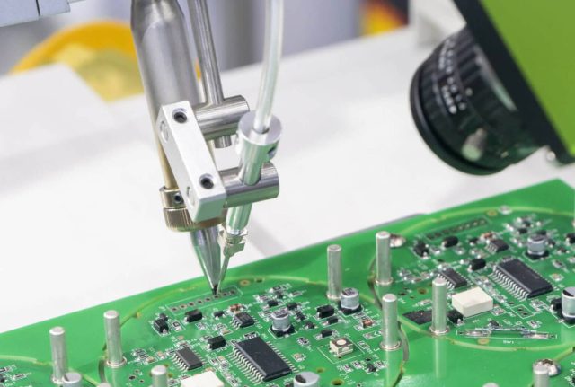
Manufacturing & Reliability Considerations
Logic Test PCB fabrication requires precision and consistency:
- Tight impedance tolerance control
- High layer registration accuracy
- Stable material selection for high-speed signals
- Durable surface finishes (ENIG, hard gold) for repeated testing
- Mechanical stability for test sockets
Reliability is critical because Logic Test PCBs are used repeatedly in production environments.
When Should You Use a Logic Test PCB?
Use a Logic Test PCB when:
- Testing high-speed digital ICs
- Validating timing and signal integrity
- Developing ATE test systems
- Working with high pin count devices
Avoid simplified designs when:
- Signal speed is high but test PCB is underdesigned
- Timing accuracy is critical
Engineering principle:Test PCB performance must match or exceed DUT requirements.
Final Thoughts
Logic Test PCBs are essential for ensuring the accuracy, reliability, and performance of digital electronic systems.
Their success depends on:
- Strong signal integrity design
- Precise timing control
- Optimized PCB architecture
- Reliable manufacturing processes
At KKPCB, we provide Logic Test PCB design and manufacturing solutions, helping customers achieve accurate digital validation and scalable production testing.
