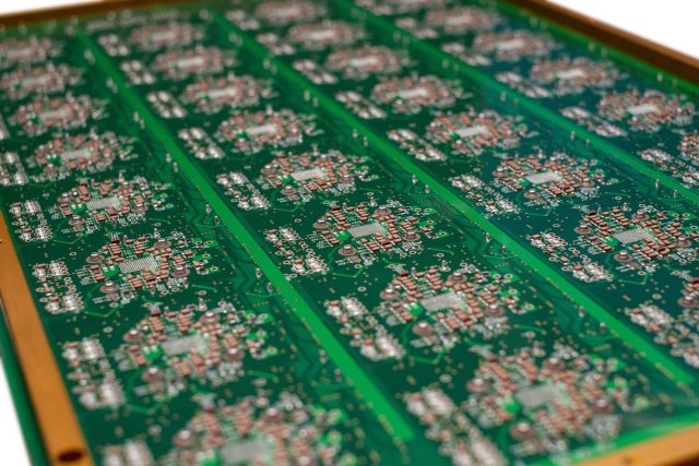
A Burn-in PCB is a printed circuit board specifically designed to support reliability testing of electronic components under elevated temperatures, voltage stress, or operational load. Burn-in testing identifies early-life failures and verifies long-term performance, making these PCBs critical for semiconductor validation, power electronics, and high-reliability systems.
Burn-in PCBs are widely used in:
-
Semiconductor testing laboratories
-
Power amplifier and IC validation
-
Aerospace and defense electronics
-
Automotive and industrial reliability testing
The goal is to simulate accelerated aging conditions to detect weak or defective components before they reach production or deployment.
Design Considerations
Designing a burn-in PCB requires careful attention to both electrical and mechanical robustness:
-
High-Temperature Components: Materials must withstand prolonged exposure to elevated temperatures without delamination or warping.
-
Uniform Power Distribution: Even heating across sockets and test sites prevents localized thermal stress.
-
Component Footprint Accuracy: Precise pad layouts for ICs, BGAs, or power devices ensure reliable insertion and contact during testing.
-
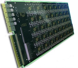
Test Connectivity: Burn-in PCBs must accommodate numerous connections for voltage, current, and monitoring circuits.
-
Layer Stack-Up: Optimized for thermal conduction, electrical isolation, and mechanical stability during thermal cycling.
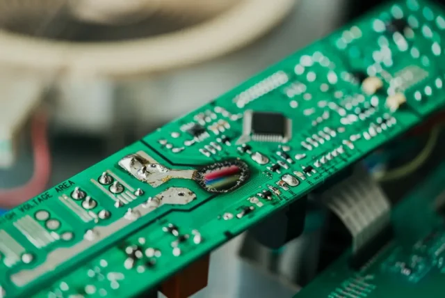
Thermal & Electrical Challenges
Burn-in PCBs face several high-stress engineering challenges:
-
Heat Management: Components generate significant heat; the board must dissipate it efficiently while maintaining uniform temperature across the test area.
-
High-Current Capacity: Some ICs or power devices require high current, necessitating reinforced traces and copper pours.
-
Signal Integrity: Testing high-speed components requires maintaining proper impedance and low noise even under thermal stress.
-
Material Stress: Repeated thermal cycling can cause cracks, delamination, or pad lift-off if materials are not carefully selected.
Fabrication & Quality Assurance
Producing burn-in PCBs requires high-reliability materials and precise manufacturing processes:
-
High-Tg Laminates: FR-4 with high glass transition temperature or BT Epoxy substrates resist thermal deformation.
-
Copper Reinforcement: Thick copper traces and planes ensure high-current capability and thermal conduction.
-
Via and Pad Reliability: Plated-through holes and via-in-pad designs maintain electrical connectivity under repeated thermal cycling.
-
Surface Finishes: ENIG, hard-gold, or immersion silver finishes improve solderability and contact reliability.
-
QA Testing:
-
Thermal profiling ensures uniform heat distribution
-
Electrical continuity and impedance checks verify circuit integrity
-
AOI/X-ray inspections detect micro-cracks, voids, or delamination
-
KKPCB applies these procedures to ensure burn-in PCBs perform reliably under repeated high-stress test conditions.
Applications
Burn-in PCBs are critical in industries that require early detection of component failures and high reliability:
-
Semiconductor Manufacturing: Testing ICs, power transistors, and microcontrollers before shipment
-
Aerospace & Defense: Validating avionics and radar components under thermal and electrical stress
-
Automotive Electronics: Ensuring ECU, ADAS, and power modules operate reliably under harsh conditions
-
High-Power Electronics: Burn-in testing of power supplies, amplifiers, and LED drivers
-
Quality Assurance Labs: Accelerated aging studies and failure analysis for electronic devices
By combining robust design, thermal management, reinforced copper, and rigorous QA, KKPCB delivers Burn-in PCBs capable of ensuring the reliability of critical components in high-stress and high-reliability applications.
