High Layer Count PCBs (printed circuit boards with 8 layers or more) have become a cornerstone in advanced electronics design. From telecommunications and medical devices to automotive and aerospace systems, these boards allow engineers to pack more functionality into smaller footprints while maintaining high performance. However, as layer counts increase, both design and manufacturing complexities grow significantly.
Design Challenges
-
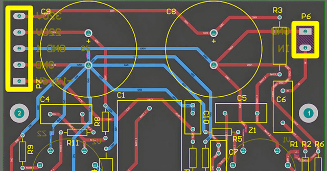
Signal Integrity:
High-speed signals are prone to interference and signal degradation. Crosstalk, reflections, and attenuation can severely affect performance. Careful trace routing, differential pair implementation, and controlled impedance design are essential to ensure reliable signal transmission. Engineers also need to manage return paths and avoid discontinuities across multiple layers. -
Impedance Control:
Consistent impedance across layers is critical, especially for RF circuits, high-speed digital communication, and mmWave modules. Even minor variations in trace width, spacing, or dielectric thickness can cause signal reflections, timing errors, or data loss. Advanced simulation and precise PCB stackup planning are essential steps to maintain impedance consistency. -
Thermal Management:
As the number of layers grows, so does the board’s heat density. Power-hungry components and dense layer stacking can cause hotspots, affecting both reliability and performance. Proper placement of thermal vias, copper planes, and heat-spreading structures is crucial. Materials with high thermal conductivity and advanced lamination techniques help mitigate overheating issues. -
Mechanical and Manufacturing Constraints:
High Layer Count PCBs require extreme precision during fabrication. Misalignment of layers, via reliability issues, and lamination defects can easily occur. Advanced techniques like sequential lamination, microvias, blind/buried vias, and precise registration help ensure structural integrity. KKPCB’s manufacturing capabilities include multi-layer lamination control, strict layer alignment, and high-quality drilling to meet these challenges.
Quality Assurance and Testing
Every layer of a complex PCB must undergo rigorous inspection. Automated Optical Inspection (AOI) detects surface defects, while X-ray inspection ensures via integrity and internal connectivity. Impedance testing verifies signal path performance, and functional testing simulates real-world conditions to confirm reliability. KKPCB applies these testing procedures to deliver boards that meet stringent industrial standards.
Applications of High Layer Count PCBs
High Layer Count PCBs are widely used in:
-
5G and Telecommunications: Supporting multi-band RF circuits, high-speed data routing, and compact module integration.
-
Automotive and ADAS Systems: Enabling advanced driver assistance systems with complex sensor networks and safety-critical functions.
-
Aerospace and Defense: Providing reliable, high-density circuitry for avionics and communication systems.
-
Industrial IoT Devices: Allowing compact yet fully featured sensor modules for data acquisition and process control.
By combining design expertise, advanced fabrication techniques, and comprehensive testing, KKPCB ensures that high layer count PCBs meet the demanding performance, reliability, and durability requirements of modern electronics.
