In today’s connected world, RF transceiver PCB design plays a critical role in enabling stable and efficient wireless communication systems. From IoT devices to advanced communication infrastructure, high-performance RF PCB design ensures signal integrity, low interference, and reliable data transmission. Understanding the key design technologies behind RF transceiver PCBs is essential for achieving optimal performance.
What Is an RF Transceiver PCB?
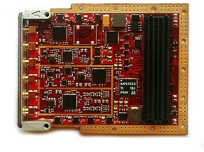
An RF transceiver PCB is a specialized printed circuit board (PCB) designed to transmit and receive radio frequency signals. Unlike standard rigid circuit boards, RF PCBs require precise layout, controlled impedance, and high-frequency materials to maintain signal quality.
These RF circuit boards are widely used in:
- Wireless communication devices
- IoT modules
- GPS systems
- Bluetooth and Wi-Fi devices
Key Design Technologies for RF Transceiver PCB
1. Controlled Impedance Design
One of the most critical aspects of RF PCB design is maintaining controlled impedance. Proper impedance matching minimizes signal reflection and ensures maximum power transfer in RF transceiver circuits.
Key considerations:
- Trace width and spacing
- Dielectric constant of materials
- Stack-up design
2. High-Frequency PCB Materials
Standard FR4 materials may not perform well at high frequencies. RF transceiver PCBs often use specialized materials such as:
- Rogers materials (e.g., RO4003C, RO4350B)
- PTFE-based laminates
These materials reduce signal loss and improve overall RF performance.
3. Signal Integrity and Layout Optimization
Maintaining signal integrity is essential in RF PCB layout. Poor layout can lead to noise, crosstalk, and signal degradation.
Best practices include:
- Short and direct RF signal paths
- Proper grounding techniques
- Isolation between RF and digital sections
4. Grounding and Shielding Techniques
Effective grounding is crucial for minimizing electromagnetic interference (EMI). RF transceiver PCB design should include:
- Continuous ground planes
- Via stitching for grounding
- Shielding structures for sensitive components
5. Thermal Management
High-frequency components generate heat, which can affect performance. Proper thermal management ensures long-term reliability of RF PCBs.
Solutions include:
- Thermal vias
- Heat sinks
- Optimized copper thickness
6. Power Supply Noise Control
Stable power delivery is essential for RF transceiver circuits. Noise in the power supply can directly impact signal quality.
Design strategies:
- Decoupling capacitors placement
- Power filtering
- Separation of analog and digital power domains
Why Choose KKPCB for RF Transceiver PCB Manufacturing?
1. Expertise in High-Frequency PCB Manufacturing
KKPCB specializes in manufacturing RF transceiver PCBs using advanced materials and precise fabrication techniques.
2. Advanced Equipment and Quality Control
With strict process control, KKPCB ensures consistent quality for high-frequency PCBs, meeting industry standards.
3. Custom RF PCB Solutions
From prototype to mass production, KKPCB offers tailored RF PCB design and manufacturing services, including multilayer RF boards.
4. Reliable Delivery and Technical Support
KKPCB provides fast turnaround times and engineering support to optimize your RF transceiver PCB design.
Applications of RF Transceiver PCBs
High-performance RF PCBs are widely used in:
- Wireless communication systems
- IoT and smart devices
- Automotive radar systems
- Satellite and GPS modules
Conclusion
Designing a high-performance RF transceiver PCB requires a deep understanding of high-frequency behavior, materials, and layout techniques. By applying key technologies such as controlled impedance, signal integrity optimization, and EMI control, engineers can achieve reliable wireless communication.
Partnering with KKPCB ensures your RF PCB projects meet the highest standards of performance, reliability, and efficiency.
