As electronic products continue to shrink in size while increasing in functionality, traditional PCB technologies face limitations in routing density and signal performance. Microvia PCB technology has emerged as a key solution for supporting high-density interconnect (HDI) designs in modern electronics.
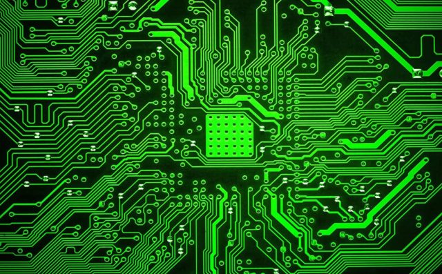
By using extremely small vias to connect circuit layers, microvia PCBs allow engineers to create compact and complex layouts that would not be possible with conventional through-hole vias.
What Is a Microvia PCB?
A microvia PCB is a printed circuit board that uses very small vias, typically with diameters less than 150 microns, to connect layers in high-density circuit designs. These microvias are usually created using laser drilling technology, which allows for precise and accurate hole formation.
Unlike traditional vias that pass through the entire board thickness, microvias generally connect only adjacent layers. This approach helps reduce signal path length and improves electrical performance.
Types of Microvia Structures
Microvia technology offers several different structures depending on the PCB design requirements.
Blind Microvias
Blind microvias connect the outer layer to an inner layer without passing through the entire board. They are commonly used in HDI designs to increase routing density.
Buried Microvias
Buried microvias connect inner layers only and are completely enclosed within the PCB structure.
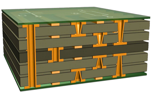
Stacked Microvias
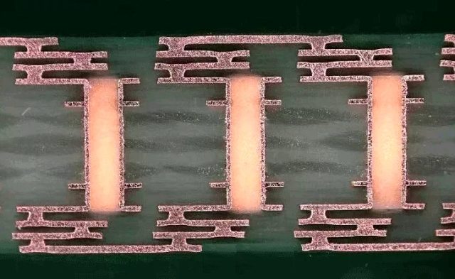
Stacked microvias are placed directly on top of each other to connect multiple layers vertically. This structure allows for very compact routing but requires precise manufacturing.
Staggered Microvias
In staggered designs, microvias are offset rather than aligned vertically. This approach improves reliability and reduces mechanical stress.
Advantages of Microvia PCB Technology
Microvia PCBs offer several important benefits for advanced electronic systems.
Higher Routing Density
Smaller vias free up valuable routing space, allowing designers to place more traces within limited board areas.
Improved Signal Integrity
Shorter signal paths reduce parasitic inductance and capacitance, which helps maintain signal quality in high-speed circuits.
Compact Product Design
Microvias enable designers to build smaller and lighter electronic devices without sacrificing functionality.
Enhanced Electrical Performance
High-frequency and high-speed circuits benefit from reduced signal distortion and improved impedance control.
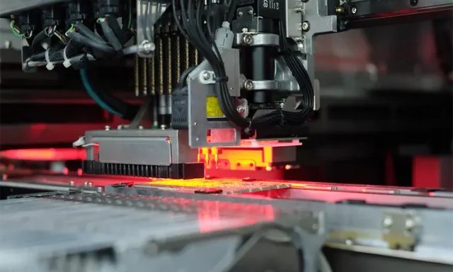
Microvia PCB Manufacturing Process
The manufacturing of microvia PCBs requires advanced fabrication technology and strict process control.
Key steps include:
-
Laser drilling to create microvias
-
Desmear and surface preparation
-
Copper plating to form electrical connections
-
Layer lamination and alignment
-
Imaging and etching of circuit patterns
-
Inspection and reliability testing
Because of the small feature sizes involved, microvia fabrication requires specialized equipment and experienced PCB manufacturers.
Applications of Microvia PCBs
Microvia PCB technology is widely used in industries that require compact, high-performance electronics.
Smartphones and Consumer Electronics
Modern mobile devices rely heavily on HDI boards with microvias to achieve compact layouts.
IoT Devices
Sensors and wireless communication modules benefit from high-density routing.
Telecommunication Equipment
High-speed data processing and communication hardware require advanced PCB structures.
Medical Electronics
Portable medical devices use microvia PCBs to reduce size while maintaining reliability.
Design Considerations for Microvia PCBs
Engineers must consider several important factors when designing microvia PCBs.
Aspect Ratio Control
Microvia depth-to-diameter ratios must remain within manufacturable limits.
Copper Filling
Stacked microvias often require copper filling to ensure reliable electrical connections.
Thermal Stress Management
Thermal expansion differences between materials must be managed to avoid microvia cracking.
Manufacturing Capabilities
Designers must confirm that the chosen PCB manufacturer supports the required microvia technology.
Conclusion
Microvia PCB technology has become an essential part of modern HDI design, enabling engineers to build compact and high-performance electronic products. By reducing via size and improving routing density, microvias support the increasing complexity of today’s electronic systems.
As demand for smaller, faster, and more powerful devices continues to grow, microvia PCBs will remain a key technology in advanced PCB manufacturing
