What Are Low Loss PCB Materials?
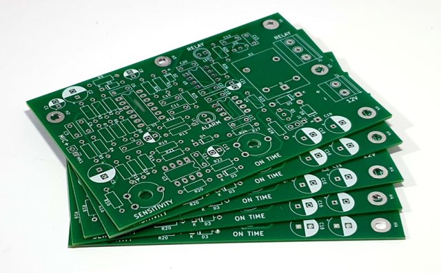
Low loss PCB materials are specialized laminate substrates designed to minimize signal attenuation during high-speed or high-frequency transmission. In modern electronic systems operating at GHz frequencies, signal loss within the dielectric material becomes a critical performance factor.
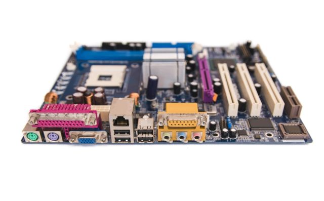
Compared to standard FR4 substrates, low loss materials feature lower dissipation factor (Df) and more stable dielectric constant (Dk), enabling improved signal integrity and transmission efficiency.
These materials are essential in RF, microwave, 5G, high-speed digital, and advanced networking applications.
Why Signal Loss Becomes Critical at High Frequency
As signal frequency increases:
-
Dielectric loss increases
-
Conductor loss becomes more significant
-
Insertion loss accumulates over trace length
-
Phase stability becomes more sensitive
Standard FR4 may perform adequately at lower frequencies, but at multi-GHz levels, dielectric loss can degrade signal quality, reduce eye diagram margin, and increase bit error rates.
Low loss materials are engineered to address these challenges.
Key Electrical Characteristics
1. Low Dissipation Factor (Df)
Lower Df means reduced dielectric energy loss. This results in:
-
Lower insertion loss
-
Improved signal amplitude retention
-
Better high-frequency efficiency
Low Df is particularly important in long trace routing and backplane applications.
2. Stable Dielectric Constant (Dk)
Consistent Dk ensures:
-
Accurate impedance control
-
Predictable signal propagation delay
-
Stable phase response across frequency
Dk stability also improves differential pair matching and timing performance.
3. Reduced Signal Attenuation
By combining low Df and stable Dk, low loss materials:
-
Minimize signal degradation
-
Improve return loss performance
-
Support higher data rates
This enables reliable operation in multi-gigabit systems.
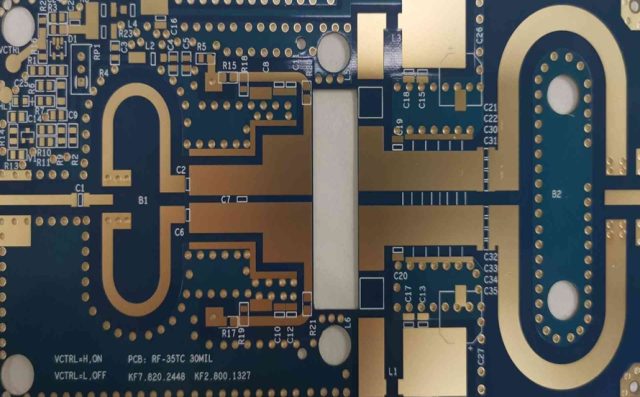
Types of Low Loss PCB Materials
Low loss PCB materials may include:
-
Enhanced FR4 with improved resin systems
-
Hydrocarbon ceramic laminates
-
PTFE-based substrates
-
High-speed digital laminate systems
-
Hybrid stack-up constructions
Material selection depends on operating frequency, cost constraints, and mechanical requirements.
Applications of Low Loss PCB Materials
Low loss substrates are widely used in:
-
5G communication infrastructure
-
High-speed backplanes
-
Data center switches and routers
-
AI computing modules
-
Automotive radar systems
-
RF power amplifiers
-
Aerospace communication systems
As data rates move beyond 10Gbps and operating frequencies exceed several GHz, low loss materials become increasingly necessary.
Low Loss vs Standard FR4
| Feature | Standard FR4 | Low Loss Material |
|---|---|---|
| Dissipation Factor | Higher | Lower |
| Frequency Performance | Moderate | High |
| Signal Attenuation | Higher | Reduced |
| Impedance Stability | Moderate | Improved |
| Cost | Lower | Higher |
Low loss materials provide measurable performance benefits in high-speed and RF environments.
Manufacturing Considerations
Fabrication using low loss materials requires:
-
Controlled lamination profiles
-
Precise dielectric thickness control
-
Impedance verification
-
Copper surface optimization
-
Careful drilling parameter adjustment
Consistent process control ensures stable electrical performance across production batches.
Conclusion
Low loss PCB materials play a vital role in enabling high-speed digital and high-frequency RF systems. By minimizing dielectric loss and stabilizing impedance characteristics, these substrates help maintain signal integrity, reduce attenuation, and support next-generation communication technologies.
For applications requiring multi-GHz performance and high data throughput, low loss materials provide a strong foundation for reliable system design.
