What Is a Multilayer Test PCB?
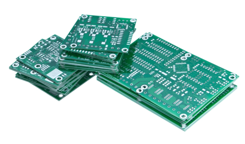
A Multilayer Test PCB is a high-layer-count printed circuit board specifically engineered for electronic testing and validation environments. It serves as a critical interface between testing equipment and the Device Under Test (DUT), ensuring accurate signal transmission and reliable measurement results.
Unlike standard multilayer PCBs used in commercial products, test PCBs are designed with a strong emphasis on electrical precision, signal integrity, repeatability, and mechanical stability.
These boards are widely used in semiconductor testing systems, high-speed validation platforms, and RF measurement setups.
Why Multilayer Structure Is Essential
Modern electronic devices—especially semiconductors and high-speed processors—require increasingly complex testing environments. Key challenges include:
- High pin-count connectivity
- Multiple power and ground references
- Controlled impedance routing
- Isolation of analog, digital, and RF signals
A multilayer structure (typically 8–30+ layers) enables:
- Dedicated ground and power planes
- Reduced electromagnetic interference (EMI)
- Stable return paths
- High-density signal routing
This architecture ensures accurate measurements and consistent signal performance during testing.
Key Technical Requirements
1. Strict Impedance Control
Multilayer test PCBs must support high-performance signal transmission, including:
- High-speed digital interfaces
- Differential pair routing
- RF transmission lines
Precise impedance control (e.g., 50Ω / 100Ω) is essential to maintain signal integrity and avoid measurement errors.
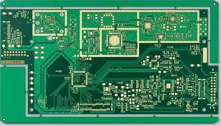
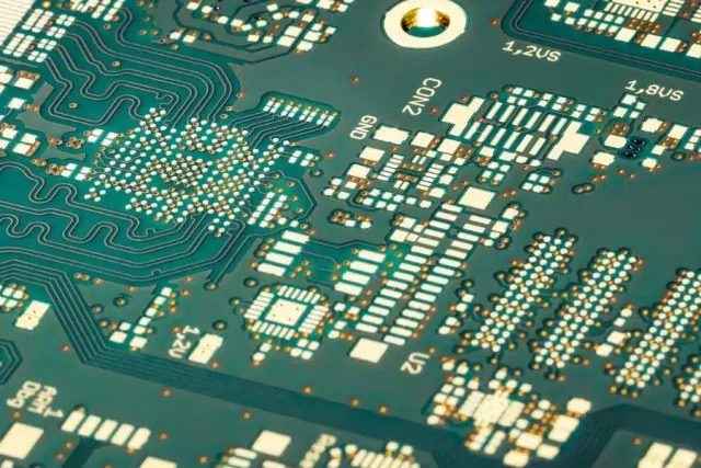
2. High Routing Density
To accommodate complex DUT packages, these boards often integrate advanced technologies such as:
- Blind and buried vias
- Microvias (HDI structures)
- Fine-pitch BGA routing
- Via-in-pad design
These features enable compact layouts with high interconnection density.
3. Mechanical Precision
Mechanical consistency is critical in testing environments. Requirements include:
- Tight dimensional tolerances
- Minimal warpage
- Accurate thickness control
- Precise socket alignment
Even small mechanical deviations can affect contact reliability and test repeatability.
4. Thermal and Current Stability
Many testing scenarios involve demanding operating conditions, such as:
- High current validation
- Continuous burn-in cycles
- Long-duration operation
To ensure stability, multilayer test PCBs may incorporate:
Effective thermal management ensures long-term reliability and consistent performance.
Applications of Multilayer Test PCB
Multilayer test PCBs are widely used across advanced electronics testing fields, including:
- Semiconductor ATE systems
- Load boards
- Burn-in boards
- Logic and functional test boards
- RF test modules
- Automotive chip validation
- High-speed processor testing
As device complexity and operating speeds increase, the demand for high-performance test PCBs continues to grow.
Multilayer Test PCB vs Standard Multilayer PCB
| Feature | Standard Multilayer PCB | Multilayer Test PCB |
|---|---|---|
| Application | End products | Testing & validation |
| Layer Count | Moderate | High |
| Impedance Control | Optional | Strict |
| Mechanical Tolerance | Standard | Tight |
| Reliability Requirement | Normal | Critical |
Test PCBs are optimized for precision, consistency, and durability, rather than product integration.
Manufacturing Capabilities
Advanced fabrication of multilayer test PCBs typically includes:
- 10–30+ layer construction
- Controlled impedance verification
- Back drilling
- HDI processing
- Low-loss materials
- X-ray and AOI inspection
- 100% electrical testing
These processes ensure stable electrical performance across repeated test cycles.
Conclusion
Multilayer Test PCBs play a vital role in modern electronic validation and semiconductor testing. Their high-layer architecture, strict impedance control, and precise mechanical design enable accurate, repeatable, and reliable testing results.
As electronic devices continue to evolve toward higher speeds and integration levels, multilayer test PCBs will remain essential in ensuring product quality and manufacturing efficiency.
