RF Test PCB – Ensuring Accurate High Frequency Testing Performance
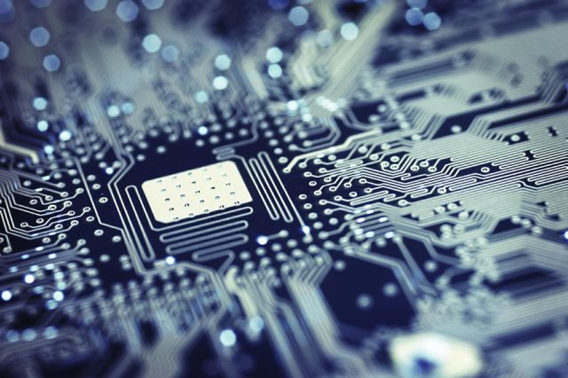
An RF Test PCB is a specialized printed circuit board designed to evaluate, validate, and characterize radio frequency (RF) components, modules, and integrated circuits. These boards are used in laboratory testing, production testing, and automated test equipment (ATE) systems to ensure RF devices meet performance specifications.
RF Test PCBs are critical for applications operating from MHz ranges to multi-GHz and even mmWave frequencies.
Why RF Test PCB Design Is Critical
At high frequencies, PCB design directly affects signal integrity and measurement accuracy. Even minor impedance mismatches, material inconsistencies, or layout errors can introduce:
-
Signal reflection
-
Insertion loss
-
Phase distortion
-
Crosstalk
-
Measurement inaccuracies
A properly engineered RF Test PCB ensures stable and repeatable testing conditions, allowing accurate device characterization.
Key design Features of RF Test PCB
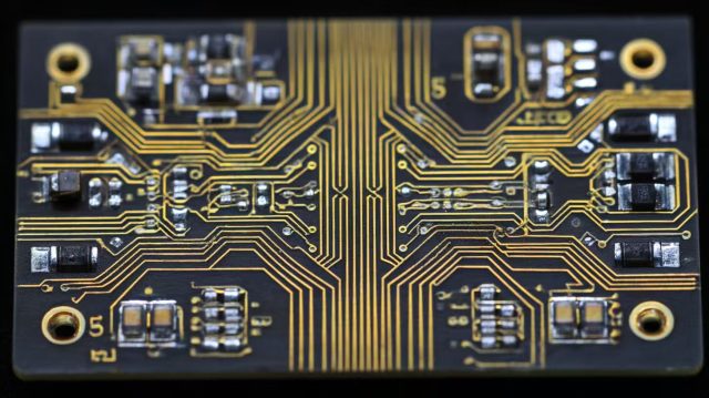
1. Controlled Impedance Routing
Precise impedance control (50Ω, 75Ω, differential pairs) is essential for maintaining signal integrity across RF transmission lines.
2. Low Loss Materials
High frequency laminates such as:
-
Rogers
-
Taconic
-
PTFE-based materials
-
Low loss hydrocarbon ceramic laminates
These materials minimize dielectric loss and maintain signal strength.
3. Optimized RF Trace design
-
Microstrip or stripline structures
-
Short signal paths
-
Smooth copper surface
-
Controlled trace width and spacing
4. Solid Ground Planes
Stable ground reference improves shielding and reduces noise.
5. High Frequency Connectors
SMA, SMP, 2.92mm (K), or other precision RF connectors are commonly integrated into RF test boards.
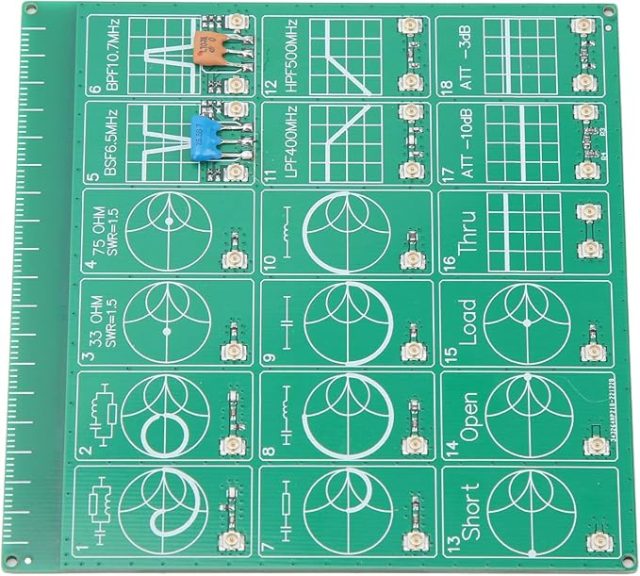
Applications of RF Test PCB
RF Test PCBs are widely used in:
-
RF IC testing
-
Power amplifier validation
-
Antenna testing
-
5G module testing
-
mmWave device evaluation
-
Satellite communication systems
-
Automotive radar testing
-
Wireless module certification
From R&D validation to high-volume production testing, RF Test PCBs play a central role in performance verification.
RF Test PCB in ATE Systems
In Automated Test Equipment (ATE), RF Test PCBs function as:
-
Load boards
-
Interface boards
-
Signal routing platforms
These boards must withstand repeated test cycles while maintaining electrical stability and mechanical durability.
Material Selection for RF Test PCB
Choosing the correct material depends on:
-
Operating frequency range
-
Loss requirements
-
Thermal performance
-
Cost considerations
For lower GHz applications, hybrid stack-ups combining FR-4 and high frequency laminates may offer cost efficiency. For mmWave applications, pure PTFE-based materials are often preferred.
Manufacturing Challenges of RF Test PCB
RF PCB fabrication requires:
-
Tight dielectric thickness control
-
Precise impedance modeling
-
Careful lamination of PTFE materials
-
Strict dimensional control
-
High-quality surface finishing
An experienced RF PCB manufacturer ensures reliable electrical performance and repeatable results.
Why Choose a Professional RF Test PCB Manufacturer
A specialized RF Test PCB supplier provides:
-
Stack-up design consultation
-
Impedance simulation support
-
Low loss material expertise
-
High frequency testing capability
-
Fast prototype turnaround
-
Stable mass production
This ensures your RF testing environment is accurate, consistent, and reliable.
