What Is a Burn-in Board PCB?
A Burn-in Board PCB is a specialized printed circuit board used in semiconductor reliability testing to identify early device failures. It connects packaged integrated circuits to burn-in test systems, allowing devices to operate under elevated temperature, voltage, and electrical stress conditions over extended periods.
Burn-in board PCBs play a critical role in ensuring long-term semiconductor reliability and are widely used in automotive electronics, aerospace, industrial control, and high-reliability communication systems.
Purpose of Burn-in Testing
Burn-in testing is designed to accelerate aging and detect early component failures before products are released to the market. A burn-in board PCB enables:
-
Continuous operation of ICs under stress conditions
-
Early failure screening and reliability verification
-
Electrical performance validation under thermal stress
-
High-volume reliability qualification testing
The durability and stability of the burn-in PCB directly impact testing accuracy and efficiency.
Key Requirements for Burn-in Board PCBs
Burn-in board PCBs must withstand extreme operating conditions and repeated test cycles. Key requirements include:
-
High temperature resistance for long burn-in cycles
-
High pin count support for complex IC packages
-
Stable power delivery and grounding
-
Controlled impedance routing for high-speed signals
-
Excellent mechanical strength and flatness
-
Long service life under thermal cycling
These requirements make burn-in PCBs significantly more demanding than standard test boards.
Design Considerations for Burn-in Board PCBs
Effective burn-in board PCB design includes:
-
Optimized multilayer stackup for thermal and electrical performance
-
Reinforced copper structures for power distribution
-
High-reliability via and pad design
-
Socket footprint optimization for thermal expansion
-
Thermal management solutions for heat dissipation
Close coordination between PCB designers, reliability engineers, and test system providers is essential.
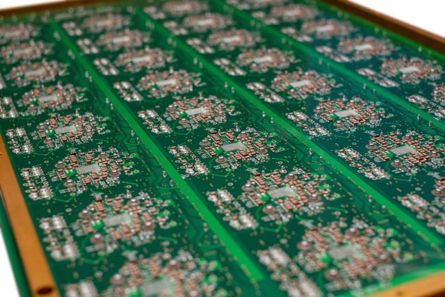
Materials Used in Burn-in Board PCBs
Burn-in board PCBs require materials that maintain electrical and mechanical stability under high temperatures. Common materials include:
-
High-TG FR-4 laminates
-
Polyimide PCB materials for extreme temperature environments
-
Low CTE materials for dimensional stability
-
High thermal performance prepregs
Material selection depends on burn-in temperature range, typically between 125°C and 200°C or higher.
Manufacturing Capabilities
A professional burn-in board PCB manufacturer should provide:
-
Multilayer PCB fabrication for complex routing
-
Controlled impedance manufacturing and validation
-
Heavy copper options for high current applications
-
Tight tolerance drilling and plating control
-
High reliability surface finishes such as ENIG or hard gold
-
Small batch and prototype manufacturing with fast delivery
Precision manufacturing ensures consistent performance during long burn-in test cycles.
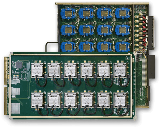
Assembly Considerations
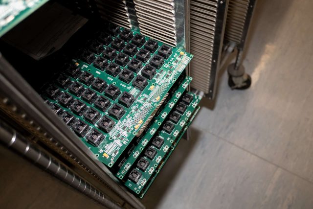
Burn-in board PCB assembly typically includes:
-
High-temperature burn-in sockets
-
Power connectors and signal interface components
-
Passive components for filtering and protection
-
Mechanical reinforcement for long-term durability
Proper assembly techniques ensure reliable electrical contact and thermal stability throughout the burn-in process.
Applications of Burn-in Board PCBs
Burn-in board PCBs are widely used in:
-
Semiconductor reliability qualification testing
-
Automotive electronics burn-in testing
-
Aerospace and defense IC reliability validation
-
Industrial and power semiconductor testing
-
High-reliability communication device screening
They are essential for ensuring product reliability in mission-critical applications.
Why Choose a Specialized Burn-in Board PCB Supplier
An experienced burn-in PCB supplier offers:
-
Expertise in high-temperature PCB materials and design
-
Stable quality for long burn-in test cycles
-
Optimized thermal and power distribution solutions
-
Fast prototype and small batch production
-
Engineering support from design review to final assembly
Selecting the right partner improves reliability screening efficiency and reduces failure risks.
