What Is a Semiconductor Load Board?
A Semiconductor Load Board is a critical interface PCB used in IC testing systems, connecting the automated test equipment (ATE) to the device under test (DUT). It provides electrical routing, signal conditioning, power delivery, and mechanical support during functional, parametric, and performance testing of semiconductor devices.
Load boards are widely used in final test, system-level test, and package-level IC testing, making them an essential component in modern semiconductor manufacturing.
Key Functions of a Semiconductor Load Board
A well-designed semiconductor load board performs multiple essential functions:
-
Routes high-speed digital signals between ATE and DUT
-
Delivers stable power and ground with low noise
-
Supports controlled impedance for signal integrity
-
Integrates passive components such as resistors and capacitors
-
Provides mechanical alignment and socket mounting
As IC complexity increases, load boards must handle higher data rates, tighter timing margins, and more demanding electrical specifications.
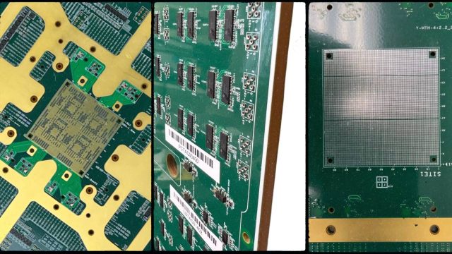
Design Challenges in Semiconductor Load Boards
Compared to standard PCBs, semiconductor load boards face unique challenges:
-
High pin count and dense routing for advanced IC packages
-
Fine pitch sockets and connectors
-
High-speed and high-frequency signal integrity control
-
Low skew and low crosstalk requirements
-
Thermal stability under continuous test cycles
-
Strict flatness and warpage control
These challenges require advanced PCB design and manufacturing capabilities.
Materials and Stackup Options
Material selection plays a vital role in load board performance. Common options include:
-
High-TG FR-4 for general-purpose IC testing
-
Low Dk / Low Df laminates for high-speed test PCB
-
Rogers, Megtron, Isola materials for RF and high-frequency applications
-
Hybrid stackups for mixed-signal load boards
For high-speed test PCB and RF IC testing, low loss materials help reduce signal attenuation and timing distortion.
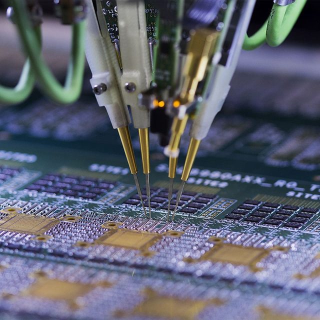
Manufacturing Capabilities for Load Board PCB
A professional semiconductor load board manufacturer should offer:
-
Multilayer PCB fabrication (often 10–30+ layers)
-
HDI technology for dense signal routing
-
Controlled impedance PCB manufacturing
-
Tight tolerance drilling and registration
-
High reliability surface finishes such as ENIG or ENEPIG
-
Small batch and prototype production with fast turnaround
Consistent quality is essential to ensure repeatable and accurate IC test results.
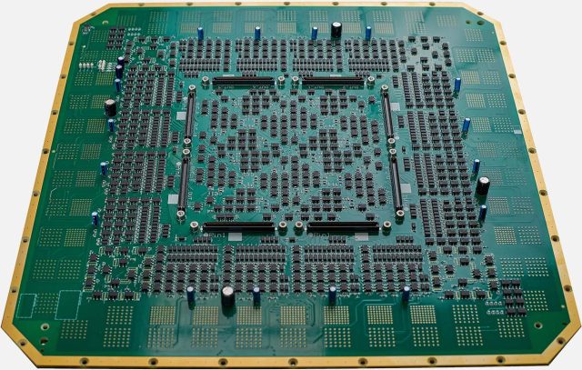
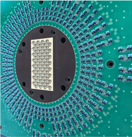
Assembly Considerations
Load board assembly typically includes:
-
IC test sockets
-
High-speed connectors
-
Discrete components for signal conditioning
-
Power filtering and decoupling networks
Precision assembly and inspection are required to maintain electrical performance and mechanical reliability throughout the test lifecycle.
Applications of Semiconductor Load Boards
Semiconductor load boards are used across a wide range of testing scenarios:
-
Final test load boards for packaged ICs
-
System-level test PCB
-
Logic IC, analog IC, and mixed-signal testing
-
Memory test PCB for DRAM and NAND devices
-
RF and high-speed IC testing platforms
They are a core element in high-volume semiconductor production environments.
Why Choose an Experienced Load Board PCB Supplier
An experienced semiconductor load board PCB supplier provides:
-
Engineering support from DFM to mass production
-
Optimized stackup and impedance control
-
High yield and long service life
-
Fast prototype and small batch delivery
-
Stable quality for repeated test cycles
Choosing the right partner directly impacts test accuracy, throughput, and overall production efficiency.
