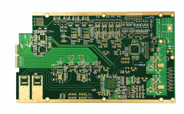
A High Speed Test PCB is a critical interface board used in automated test equipment (ATE) and semiconductor testing systems. As data rates increase and device nodes continue to shrink, high speed test PCBs must support multi-gigabit signal transmission while maintaining excellent signal integrity, impedance accuracy, and electrical stability.
Compared with standard test boards, high speed test PCBs are engineered specifically for high-frequency, high-speed digital, and mixed-signal testing environments.
What Is a High Speed Test PCB?

A High Speed Test PCB connects the ATE system to the device under test (DUT), enabling accurate measurement of electrical performance under real operating conditions. These PCBs handle fast edge rates, high pin counts, and dense routing while minimizing signal loss, reflection, and crosstalk.
They are widely used in wafer sort, final test, and system-level semiconductor testing.
Key Features of High Speed Test PCB
Controlled Impedance
Precise impedance control is essential for maintaining signal integrity in high speed test PCBs, especially for differential pairs and high-speed serial interfaces.
Low Loss Signal Transmission
Low Dk and low Df materials are used to reduce insertion loss and timing skew at high frequencies.
High Layer Count Structure
High speed test PCBs often require multilayer stack-ups with dedicated signal, power, and ground planes to support complex routing.
High Pin Count Support
Designed to accommodate fine-pitch connectors, sockets, and high-density DUT interfaces.
Materials for High Speed Test PCB
To meet performance requirements, high speed test PCBs commonly use:
-
High-performance FR-4 (for moderate speeds)
-
Rogers RO4350B, RO4835, RO4003
-
Megtron 6 / Megtron 7
-
Taconic high speed laminates
-
Hybrid material stack-ups
Material selection depends on test frequency, data rate, and reliability requirements.
Manufacturing Capabilities
Professional High Speed Test PCB manufacturing includes:
-
Tight trace width and spacing control
-
Controlled impedance fabrication and testing
-
Multilayer, HDI, blind via, and buried via processes
-
Back drilling for signal integrity improvement
-
High precision registration and drilling
These capabilities ensure consistent electrical performance across all test boards.
High Speed Test PCB Assembly
Assembly quality is equally important for high speed test PCBs. Key assembly considerations include:
-
Fine-pitch and high pin count component placement
-
Precision connector and socket installation
-
Controlled solder profiles to prevent warpage
-
AOI, X-ray inspection, and electrical testing
High-quality assembly ensures the designed signal performance is fully preserved.
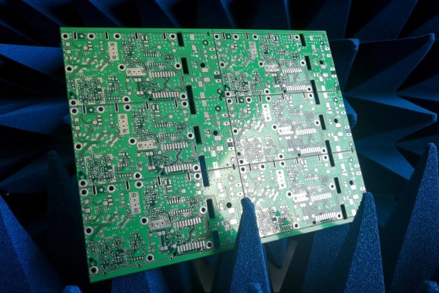
Applications of High Speed Test PCB
High speed test PCBs are widely used in:
-
ATE load boards
-
Semiconductor wafer sort and final test
-
High speed logic and memory testing
-
RF and mixed-signal IC testing
-
Automotive and high-reliability device validation
In these applications, test accuracy directly affects yield and production efficiency.
Prototype and Volume Production
Most projects start with high speed test PCB prototypes to validate impedance, loss, and signal integrity. Once verified, designs can transition smoothly into low-volume or mass production with strict process control.
Working with an experienced high speed test PCB manufacturer reduces development risk and shortens test system deployment time.
Conclusion
A High Speed Test PCB is essential for modern semiconductor and ATE testing. Through advanced materials, controlled impedance design, precision manufacturing, and reliable assembly, high speed test PCBs ensure accurate, stable, and repeatable testing results.
Choosing a capable supplier guarantees long-term performance and reliability in demanding high-speed test environments.
