A Custom ATE PCB is a critical interface component designed specifically for automated test equipment (ATE) used in semiconductor and electronic device testing. Unlike standard PCBs, custom ATE PCBs are engineered to meet unique electrical, mechanical, and reliability requirements defined by the test system, device under test (DUT), and test environment.
With increasing device complexity, higher signal speeds, and tighter test tolerances, custom ATE PCB solutions have become essential for accurate, repeatable, and high-throughput testing.
What Is a Custom ATE PCB?
A Custom ATE PCB is a tailor-made printed circuit board designed according to specific ATE system requirements. It serves as the electrical and mechanical interface between the ATE platform and the DUT, enabling signal routing, power delivery, measurement access, and control functions.
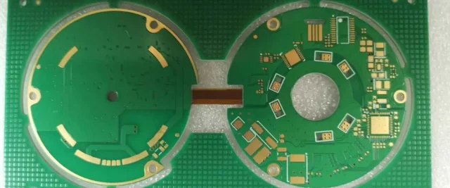
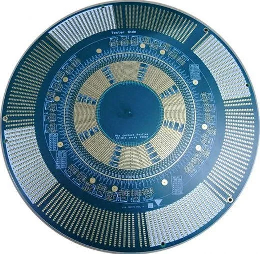
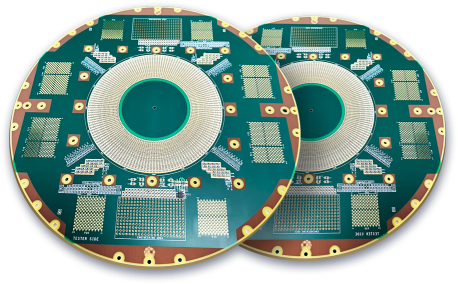
Custom ATE PCBs are commonly used as load boards, test interface boards, or application-specific test fixtures, where standard PCB designs cannot meet performance or durability needs.
Why Custom ATE PCB Design Is Essential
Application-Specific Signal Requirements
ATE systems often handle a mix of high-speed digital, analog, and RF signals. Custom ATE PCB design ensures optimized routing, isolation, and impedance control for each signal type.
Precise Controlled Impedance
Accurate impedance matching is critical for minimizing signal reflection and measurement error. Custom stack-up and trace geometry are designed to meet exact impedance targets.
Mechanical Durability
Custom ATE PCBs must withstand repeated connector mating, probing, and mechanical stress over thousands of test cycles.
Thermal Stability
High-power testing generates heat. Custom PCB designs incorporate appropriate materials and copper structures to maintain thermal and electrical stability.
Materials Used in Custom ATE PCB Manufacturing
Material selection is driven by signal speed, durability, and test environment:
-
High-Tg FR-4 for standard ATE applications
-
Low-loss laminates for high-speed and RF testing
-
Hybrid stack-ups combining FR-4 with high-frequency materials
-
Thick copper constructions for power and stress testing
An experienced custom ATE PCB manufacturer assists in selecting materials that balance performance, longevity, and cost.
Manufacturing Capabilities for Custom ATE PCBs
Producing reliable custom ATE PCBs requires advanced manufacturing processes and strict quality control:
-
Multilayer and high layer count PCB fabrication
-
Controlled impedance PCB manufacturing
-
Fine line and space etching
-
Robust via plating for long test life
-
Surface finishes such as ENIG or hard gold for test interfaces
-
Electrical testing and impedance verification
These capabilities ensure consistent performance in demanding ATE environments.
Design Support and Engineering Collaboration
Custom ATE PCB projects benefit greatly from early engineering involvement:
-
Stack-up and impedance optimization
-
High-density routing for large pin-count DUTs
-
Connector, socket, and probe interface integration
-
Signal integrity and crosstalk control
-
EMI shielding and grounding strategies
Close collaboration between the customer and the PCB manufacturer improves first-pass success and reduces development cycles.
Applications of Custom ATE PCBs
Custom ATE PCBs are widely used in:
-
Semiconductor wafer testing
-
IC package and final test
-
Logic and functional testing
-
Burn-in and reliability testing
-
Automotive and industrial electronics validation
-
High-speed and high-frequency device testing
In these applications, PCB performance directly impacts test accuracy and system uptime.
From Prototype to Volume Production
Custom ATE PCB development typically starts with prototype builds to validate electrical performance, mechanical strength, and connector reliability. Once approved, designs are transitioned to small-batch or volume production using consistent materials and controlled processes.
Working with a single supplier from prototype through production ensures continuity and long-term supply stability.
Conclusion
A Custom ATE PCB is a mission-critical component for automated test equipment and semiconductor validation systems. By combining application-specific design, precise impedance control, and high-reliability manufacturing, professional PCB suppliers deliver custom ATE PCBs that ensure accurate, repeatable, and long-lasting test performance.
As test requirements continue to evolve, choosing an experienced custom ATE PCB manufacturer is essential for supporting advanced testing technologies and scalable production.
