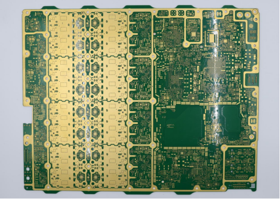
Introduction to ATE Test PCB

ATE Test PCB (Automated Test Equipment Test PCB) is a specialized printed circuit board designed to support automated electronic testing systems. An ATE Test PCB plays a critical role in verifying the electrical performance, reliability, and functionality of semiconductor devices, integrated circuits, and electronic modules during production and quality control processes.
With the rapid advancement of semiconductor technology, high-speed communication systems, and complex electronic products, the demand for high-precision ATE Test PCB solutions continues to grow. Manufacturers require ATE Test PCBs that deliver excellent signal integrity, stable impedance control, and long-term durability to ensure accurate test results and efficient mass production.
Key Functions of ATE Test PCB
An ATE Test PCB serves as the interface between the testing system and the device under test (DUT). These boards are engineered to support complex testing requirements and provide reliable electrical connections.
1. Signal Transmission Accuracy
ATE Test PCBs ensure high-frequency and high-speed signal transmission without distortion. Precise routing and impedance control are essential to maintain signal integrity during testing.
2. Device Performance Verification
ATE Test PCBs allow automated test equipment to verify electrical parameters such as voltage, current, timing, and signal performance.
3. Multi-Channel Testing Capability
Modern ATE Test PCBs support multi-channel and high-density testing environments, improving testing efficiency and reducing production costs.
4. Thermal and Mechanical Stability
ATE Test PCBs are designed to withstand repeated testing cycles and high operating temperatures while maintaining stable electrical performance.
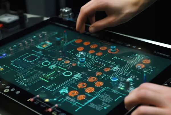
ATE Test PCB Design Requirements
Designing a high-performance ATE Test PCB requires advanced engineering expertise and strict quality control standards.
High-Density Interconnect Design
ATE Test PCBs often require HDI structures to accommodate dense test points and complex routing. Blind vias, buried vias, and microvias are commonly used to achieve compact designs.
Controlled Impedance Routing
Maintaining accurate impedance control is essential for high-speed ATE Test PCB applications. Proper stack-up design and material selection help minimize signal reflection and loss.
High Layer Count Structure
ATE Test PCBs frequently use multilayer structures to support complex signal routing, power distribution, and shielding requirements.
Precision Pad and Probe Interface Design
ATE Test PCBs must ensure reliable contact with test probes and sockets, requiring tight manufacturing tolerances and consistent surface finishing.
Materials Used in ATE Test PCB Manufacturing
Material selection significantly impacts the performance and reliability of an ATE Test PCB. High-quality materials help ensure stable signal transmission and thermal performance.
High-Frequency Laminates
Materials such as Rogers, Taconic, and other low-loss laminates are commonly used in high-speed ATE Test PCB applications.
Low Loss and Low Dk Materials
Low dielectric constant (Dk) and low dissipation factor (Df) materials help reduce signal attenuation and improve high-frequency performance.
High Tg FR-4 Materials
For standard ATE Test PCB applications, high Tg FR-4 materials provide improved thermal resistance and mechanical stability.
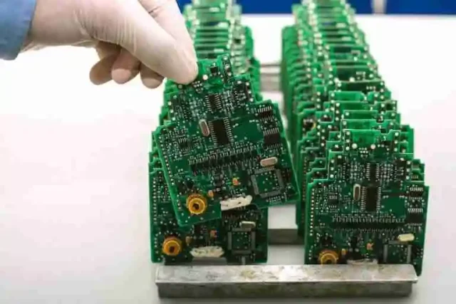
Manufacturing Challenges of ATE Test PCB
Producing reliable ATE Test PCBs requires advanced manufacturing capabilities and strict quality control.
Tight Tolerance Drilling
ATE Test PCBs often include thousands of test points and microvias, requiring high-precision drilling technology.
Fine Line and Space Capability
High-density ATE Test PCBs demand fine trace widths and spacing to support complex routing requirements.
Surface Finish Selection
Surface finishes such as ENIG, hard gold, and immersion silver are commonly used to improve durability and contact reliability.
Signal Integrity Testing
Manufacturers must perform impedance testing, electrical testing, and reliability validation to ensure ATE Test PCB performance.
Applications of ATE Test PCB
ATE Test PCBs are widely used across multiple high-tech industries.
Semiconductor Testing
ATE Test PCBs are essential for wafer testing, IC validation, and package-level testing in semiconductor manufacturing.
Telecommunications and 5G Equipment
ATE Test PCBs support high-frequency testing for 5G modules, RF devices, and communication infrastructure.
Automotive Electronics
ATE Test PCBs are used in testing ADAS systems, vehicle communication modules, and power electronics.
Consumer Electronics
ATE Test PCBs ensure quality and reliability testing for smartphones, wearable devices, and smart home electronics.
Industrial and Aerospace Applications
ATE Test PCBs are critical in testing industrial control systems, satellite electronics, and defense communication equipment.
Advantages of High-Quality ATE Test PCB Solutions
Choosing a reliable ATE Test PCB manufacturer provides several advantages:
-
Improved testing accuracy and reliability
-
Enhanced signal integrity and impedance control
-
Increased testing efficiency and reduced production downtime
-
Long-term durability for repeated testing cycles
-
Support for advanced semiconductor and high-frequency applications
Conclusion
ATE Test PCB technology plays a vital role in modern electronic manufacturing and semiconductor testing. A well-designed and precisely manufactured ATE Test PCB ensures accurate device validation, stable signal performance, and efficient automated testing operations. As electronic products continue to evolve toward higher speed and complexity, the demand for advanced ATE Test PCB solutions will continue to grow across industries.
