What Is a Buried Via PCB?
A Buried Via PCB is a multilayer printed circuit board that uses vias connecting only internal layers without reaching the outer surface layers. These hidden interconnections allow designers to increase routing density while maintaining surface space for components and signal traces.
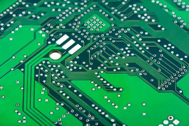
Buried Via PCBs are widely used in HDI PCB technology and advanced electronic systems that require compact design and high signal performance.
Buried Via PCB Structure
In a Buried Via PCB, vias are formed between selected internal copper layers during sequential lamination. Unlike through-hole vias, buried vias remain entirely inside the board structure.
A typical buried via configuration includes:
-
Internal layer-to-layer electrical connection
-
Multiple lamination cycles
-
HDI microvia integration
-
Optimized multilayer stack-up design
This structure improves routing efficiency while reducing signal interference.
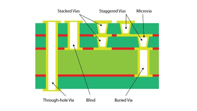
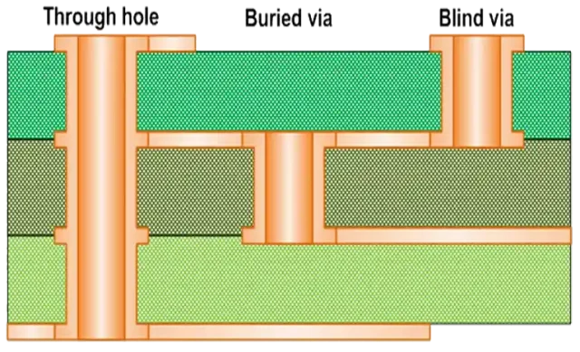
Buried Via PCB vs Other Via Types
Buried Via
-
Connects internal layers only
-
Does not appear on PCB surface
-
Improves routing density
Blind Via
-
Connects outer layer to internal layer
-
Visible on one PCB surface
Through-Hole Via
-
Connects all layers
-
Easiest to manufacture but consumes routing space
Buried Via PCB technology is essential for high-density circuit design.
Advantages of Buried Via PCB
Buried Via PCBs provide several technical benefits:
Higher Routing Density
Internal layer interconnections free surface routing space for components and high-speed signals.
Improved Signal Integrity
Shorter signal paths reduce transmission loss and signal distortion.
Reduced Electromagnetic Interference
Optimized via structures improve EMI control and reduce crosstalk.
Enhanced Electrical Performance
Internal connections provide stable signal transmission for high-speed designs.
Compact PCB Layout
Buried vias enable smaller board size and higher functional integration.
Manufacturing Process of Buried Via PCB
Producing Buried Via PCBs requires advanced fabrication techniques:
-
Sequential lamination process
-
Precision drilling or laser microvia drilling
-
Internal layer plating technology
-
High accuracy layer alignment
-
Electrical testing and reliability verification
Manufacturing buried via PCBs demands strict process control and advanced engineering expertise.
Design Considerations for Buried Via PCB
Successful buried via PCB design requires attention to:
-
Stack-up structure planning
-
Via size and aspect ratio optimization
-
Signal integrity and impedance control
-
Thermal expansion management
-
Lamination cycle design
-
Manufacturability and yield optimization
Early collaboration with PCB manufacturers helps ensure reliable production.
Applications of Buried Via PCB
Buried Via PCBs are widely used in advanced electronic applications such as:
-
Smartphones and mobile communication devices
-
5G network equipment
-
AI computing and high-performance processors
-
Aerospace and defense electronics
-
Medical imaging and wearable medical devices
-
Automotive ADAS and radar modules
-
Semiconductor test equipment
-
High-speed data communication systems
Conclusion
A Buried Via PCB is a critical technology for modern HDI and multilayer PCB designs, enabling higher routing density, improved signal integrity, and compact electronic systems. With advanced sequential lamination and precision manufacturing processes, buried via PCBs support complex and high-performance electronic applications.
Working with an experienced Buried Via PCB manufacturer ensures accurate via formation, reliable layer bonding, and consistent electrical performance.
