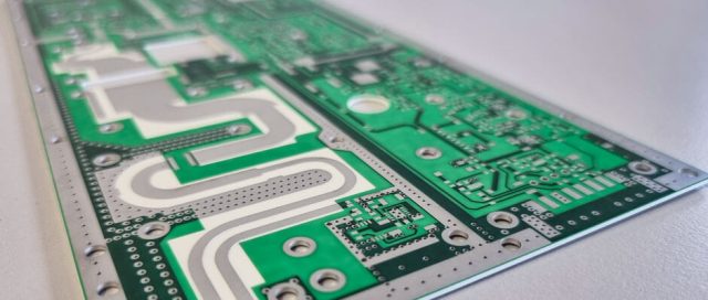
What Is a Double Layer HF PCB?
A Double Layer HF PCB (High Frequency PCB) is a two-layer printed circuit board specifically designed for RF and microwave signal transmission. It uses low dielectric loss materials and optimized trace layouts to maintain signal integrity at high operating frequencies.
Compared with multilayer RF boards, double layer HF PCBs offer a simpler structure, lower cost, and stable electrical performance, making them widely used in medium-frequency RF applications.
Structure of Double Layer HF PCB
A typical Double Layer HF PCB consists of:
-
Top RF signal layer
-
High-frequency dielectric substrate
-
Bottom ground or signal layer
This simple stack-up allows excellent signal referencing and impedance control when designed properly.
Key Electrical Characteristics
Double Layer HF PCBs are designed to provide:
-
Stable dielectric constant (Dk)
-
Low dissipation factor (Df)
-
Controlled impedance
-
Low insertion loss
-
Excellent signal stability
-
Minimal phase distortion
These characteristics are essential for maintaining RF signal quality.
Common Materials for Double Layer HF PCB
Material selection plays a critical role in high-frequency performance. Common materials include:
-
Rogers RO4350B
-
Rogers RO4003C
-
Rogers RO4835
-
Taconic RF-35
-
Taconic TLY-5
-
PTFE-based laminates
-
Hybrid HF + FR-4 structures
These materials provide low dielectric loss and stable electrical properties across wide frequency ranges.
Design Considerations
Proper design is essential to achieve reliable RF performance. Important factors include:
Controlled Impedance
Accurate trace width and spacing ensure signal matching and reduce reflections.
Ground Plane Integrity
Continuous ground planes help minimize electromagnetic interference and maintain signal reference stability.
Trace Routing Optimization
Short, smooth RF traces reduce signal attenuation and radiation loss.
Copper Surface Roughness Control
Low-profile copper foil helps reduce conductor loss at high frequencies.
Manufacturing Requirements
Producing Double Layer HF PCBs requires strict process control, including:
-
High precision lamination process
-
Tight dielectric thickness tolerance
-
Advanced drilling and plating technology
-
Impedance testing and verification
-
Clean fabrication environment for RF laminates
Applications of Double Layer HF PCB
Double Layer HF PCBs are widely used in:
-
RF communication modules
-
Wireless antenna systems
-
5G RF front-end circuits
-
High-frequency sensor PCBs
-
Radar and ADAS modules
-
Satellite communication equipment
-
Industrial RF control systems
-
IoT wireless communication devices
Advantages of Double Layer HF PCB
Compared with multilayer HF PCBs, double layer structures offer:
-
Lower manufacturing cost
-
Faster production turnaround
-
Simpler stack-up design
-
High reliability
-
Easier impedance control
-
Suitable for medium-complexity RF circuits
Conclusion
A Double Layer HF PCB provides an efficient and cost-effective solution for RF and high-frequency electronic systems. By selecting low-loss materials, optimizing layout design, and applying advanced manufacturing techniques, double layer HF PCBs deliver stable and reliable high-frequency performance.
Working with an experienced HF PCB manufacturer ensures accurate impedance control, consistent dielectric properties, and dependable production quality.
