What Is a High Frequency Sensor PCB?

A High Frequency Sensor PCB is a specialized printed circuit board engineered for high-frequency signal processing in sensors, such as radar, LiDAR, mmWave, and RF sensing modules.
These PCBs are designed to maintain signal integrity, minimize insertion loss, and provide accurate impedance control, which are critical for precise sensor measurement and reliable system performance.
Key Requirements for High Frequency Sensor PCB
High Frequency Sensor PCBs must meet strict technical requirements:
-
Low dielectric loss (Df) for high-frequency signals
-
Stable dielectric constant (Dk) for consistent impedance
-
Controlled impedance (50Ω, 75Ω, or custom)
-
High signal integrity and minimal crosstalk
-
Thermal stability for outdoor or harsh environments
-
Reliable connector and interconnect interfaces
These requirements ensure precise sensor signal acquisition and processing.
Material Selection for High Frequency Sensor PCB
Material choice is crucial for performance:
-
RO4835, RO4350B, RF-35 laminates – for RF and microwave sensors
-
Megtron 7 / Low-loss FR-4 hybrid materials – for high-speed digital sensor circuits
-
Rigid-flex or ceramic substrates – for compact and thermally stable modules
Selecting the right material ensures low insertion loss and high measurement accuracy.
Design Considerations for High Frequency Sensor PCB
Key design considerations include:
-
Short, direct RF signal paths
-
Optimized ground and power planes
-
Via fencing and isolation for RF signals
-
Precise impedance control for transmission lines
-
Connector launch optimization
-
Thermal management for high-frequency modules
Proper design ensures reliable performance across the sensor’s operating frequency range.
Manufacturing Challenges of High Frequency Sensor PCB
Producing High Frequency Sensor PCBs requires:
-
Tight dielectric and layer thickness tolerance
-
Controlled copper roughness
-
High-precision multilayer registration
-
Strict impedance and insertion loss testing
-
Advanced surface finishing for RF performance
Experienced PCB manufacturers are critical for delivering consistent sensor PCB quality.
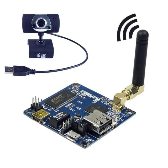
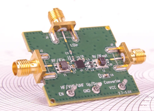
Applications of High Frequency Sensor PCB
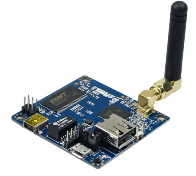
High Frequency Sensor PCBs are widely used in:
-
Automotive radar and LiDAR modules (ADAS systems)
-
5G mmWave sensors
-
Industrial and environmental RF sensors
-
Medical imaging sensors
-
IoT and smart sensor devices
-
High-frequency test and measurement modules
They are essential for precise high-speed sensing and measurement.
Conclusion
A High Frequency Sensor PCB is essential for high-accuracy, high-speed sensor systems. By combining low-loss materials, precise impedance control, and advanced manufacturing processes, these PCBs ensure reliable performance in automotive, industrial, communication, and IoT applications.
Partnering with a professional High Frequency Sensor PCB manufacturer guarantees stable RF performance, high signal integrity, and repeatable measurement results from prototype to mass production.
