What Is a Burn-in PCB?
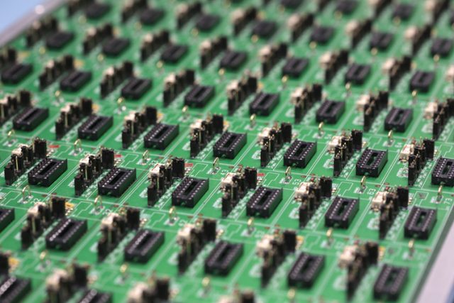
A Burn-in PCB is a specialized printed circuit board used for burn-in testing, where electronic components or assemblies are operated under elevated temperature, voltage, and current conditions for an extended period. The purpose of a Burn-in PCB is to identify early-life failures and verify long-term reliability before products enter mass production.
Compared with standard PCBs, Burn-in PCBs are designed to withstand continuous thermal stress, high current loads, and repeated test cycles without electrical or mechanical degradation.
Key Design Requirements for Burn-in PCB
Reliable Burn-in PCB design is critical to successful stress testing. Key requirements include:
-
High thermal resistance
Stable performance under elevated temperatures and long-duration testing. -
High-current capability
Wide traces, thick copper, and robust vias to handle continuous current flow. -
Efficient thermal management
Copper planes, thermal vias, or metal-core structures for heat dissipation. -
Mechanical durability
Resistance to warpage and fatigue from repeated insertion into burn-in systems. -
Stable electrical characteristics
Minimal resistance change under temperature and load variations.
These design factors ensure consistent and repeatable burn-in test results.
Materials Used in Burn-in PCB
Material selection is critical for Burn-in PCB reliability:
-
High-Tg FR-4 laminates
Suitable for moderate temperature burn-in testing. -
Metal-Core PCBs (MCPCB)
Excellent thermal performance for high-power burn-in applications. -
Ceramic PCBs
Superior thermal stability and low expansion for demanding environments. -
High-reliability hybrid materials
Used when both thermal and electrical performance are required.
Choosing the right materials ensures long service life during repeated burn-in cycles.
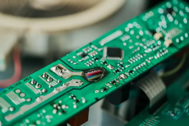
Burn-in PCB Manufacturing Considerations
Manufacturing a Burn-in PCB requires stricter process control than standard PCBs:
-
Thick copper plating and reinforced vias
-
Precise lamination and layer alignment
-
High-temperature-resistant solder mask
-
Durable surface finishes
ENIG, hard gold, or immersion silver for stable contact performance. -
Electrical and thermal reliability testing
Experienced Burn-in PCB manufacturers ensure boards remain stable throughout extended stress testing.
Advantages of Using Burn-in PCB
Using a dedicated Burn-in PCB provides key advantages:
-
Early detection of latent defects
-
Improved product reliability and yield
-
Reduced field failure and warranty risk
-
Consistent and repeatable stress test conditions
-
Compliance with strict quality and reliability standards
Burn-in PCBs play a critical role in quality assurance for high-reliability electronics.
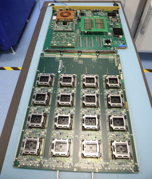
Applications of Burn-in PCB
Burn-in PCBs are widely used in industries requiring high reliability:
-
Semiconductor and IC burn-in testing
-
Power electronics and automotive modules
-
Medical electronics reliability verification
-
Telecommunication and networking equipment
-
Industrial and aerospace electronics
They are essential wherever products must operate reliably under harsh conditions.
Burn-in PCB vs Standard Test PCB
Compared to standard test PCBs, Burn-in PCBs feature:
-
Higher thermal resistance
-
Greater current-carrying capability
-
Stronger mechanical durability
-
Longer operational life under stress
These differences make Burn-in PCBs uniquely suited for accelerated aging tests.
Conclusion
A Burn-in PCB is a critical tool for accelerated stress testing and long-term reliability verification of electronic products. From high-temperature materials and thick copper design to precise manufacturing control, every detail affects burn-in performance.
Choosing an experienced Burn-in PCB supplier ensures stable, durable, and high-quality boards capable of supporting demanding burn-in environments and improving overall product reliability.
