What Is an RF Test PCB?
An RF Test PCB is a specialized printed circuit board designed specifically for accurate RF and microwave signal testing. It is widely used to evaluate RF circuits, modules, and components under real operating conditions, ensuring reliable measurement results.
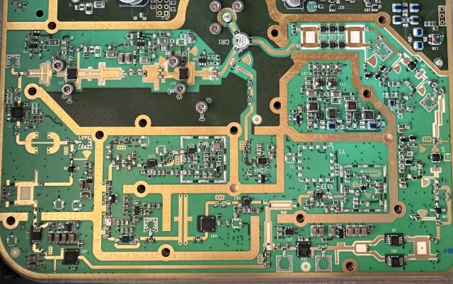
Unlike standard PCBs, an RF Test PCB is optimized for high-frequency signal integrity, featuring controlled impedance transmission lines, low-loss materials, and precise geometries. These characteristics make RF Test PCBs essential for validating parameters such as insertion loss, return loss, phase stability, and impedance matching.
In RF and microwave testing environments, even minor PCB variations can significantly affect measurement accuracy—making RF Test PCB design and manufacturing critical.
Key Design Considerations for RF Test PCB
Proper RF Test PCB design is essential to minimize signal distortion and measurement errors. Key design considerations include:
-
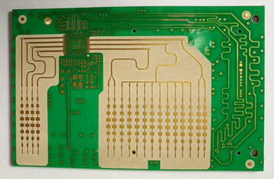
Controlled impedance routing
RF Test PCBs typically require 50Ω or 75Ω impedance control with tight tolerances. -
Consistent transmission line geometry
Uniform trace width, spacing, and reference planes ensure stable RF performance. -
Optimized via transitions
Reduced via stubs and strategically placed ground vias improve signal continuity. -
Precision connector launches
Accurate SMA, SMP, or 2.92 mm connector footprints are critical for RF Test PCB accuracy. -
Robust grounding strategy
Continuous ground planes and stitching vias help suppress EMI and noise.
These RF Test PCB design practices help ensure repeatable and trustworthy RF measurements.
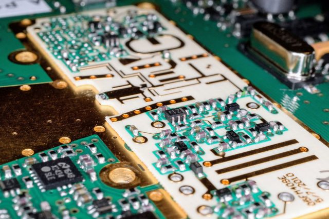
Materials Selection for RF Test PCB
Material choice plays a decisive role in RF Test PCB performance. High-frequency testing demands materials with low dielectric loss and stable dielectric constant (Dk).
Common RF Test PCB materials include:
-
Rogers laminates (RO4350B, RO4003C, RT/duroid series)
Widely used for RF Test PCBs due to low loss and excellent frequency stability. -
PTFE-based materials
Ideal for microwave and millimeter-wave RF Test PCB applications. -
High-performance FR-4 (limited use)
Suitable for lower-frequency RF Test PCBs when cost sensitivity is a factor.
Selecting the right RF Test PCB material ensures accurate signal transmission and consistent test results.
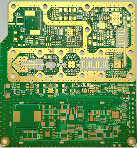
RF Test PCB Manufacturing Requirements
Manufacturing an RF Test PCB requires significantly higher precision than standard PCB fabrication. Critical manufacturing requirements include:
-
Tight impedance tolerance control
RF Test PCBs often require impedance accuracy within ±5% or tighter. -
High-precision etching processes
Ensures consistent trace width and spacing for RF signal paths. -
Smooth copper surface finishes
Reduce conductor loss and skin effect at high frequencies. -
Accurate layer alignment
Essential for multilayer RF Test PCB designs. -
Comprehensive electrical and RF testing
Verifies impedance, continuity, and overall RF performance.
Close coordination between RF designers and RF Test PCB manufacturers is crucial to achieving reliable results.
Advantages of Using RF Test PCB
Using a dedicated RF Test PCB offers several key advantages:
-
High measurement accuracy and repeatability
-
Reduced signal reflection and transmission loss
-
Improved RF signal integrity
-
Reliable evaluation of RF components and modules
-
Greater confidence in final product validation
A well-designed RF Test PCB ensures that test results accurately reflect actual RF circuit behavior.
Applications of RF Test PCB
RF Test PCBs are widely used across high-frequency and wireless industries, including:
-
RF module and antenna testing
-
5G and wireless communication systems
-
Microwave and millimeter-wave component evaluation
-
Automotive radar and ADAS testing
-
Aerospace and defense RF validation
As RF frequencies continue to increase, the demand for high-performance RF Test PCBs continues to grow.
Conclusion
An RF Test PCB is a critical tool for achieving accurate, repeatable, and reliable RF measurements. From material selection and impedance control to manufacturing precision, every detail directly impacts RF test accuracy.
Choosing an experienced RF Test PCB manufacturer with strong high-frequency expertise ensures consistent performance, reduced test uncertainty, and dependable validation results for advanced RF applications.
