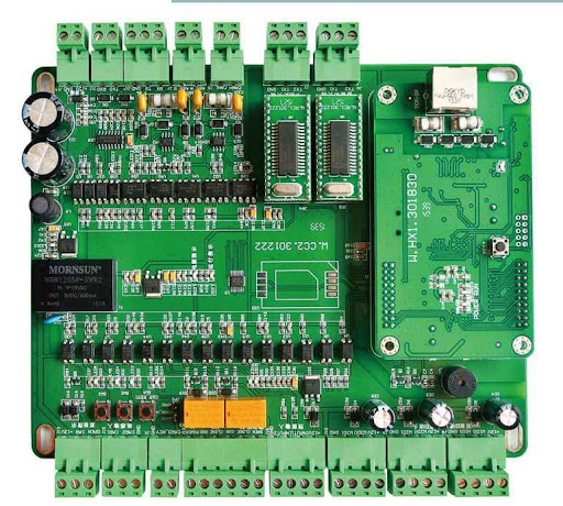
An IoT IC Test PCB is a purpose-built printed circuit board designed to support functional testing, performance validation, and reliability verification of IoT integrated circuits. As IoT devices integrate wireless communication, low-power processing, sensors, and mixed-signal interfaces, the IoT IC test PCB plays a critical role in ensuring device accuracy, stability, and mass-production readiness.
Key Features of IoT IC Test PCBs

A high-quality IoT IC Test PCB must support diverse electrical and environmental requirements:
-
Low-power signal integrity for battery-powered IoT chips
-
Support for RF, Bluetooth, Wi-Fi, Sub-GHz, NB-IoT, and LoRa testing
-
Mixed-signal testing for analog sensors and digital logic
-
Controlled impedance routing for RF and high-speed interfaces
-
Fine-pitch and high pin count IC support
-
Stable power distribution and noise isolation
These features ensure reliable and repeatable test results throughout development and production.
Applications of IoT IC Test PCBs
IoT IC Test PCBs are widely used across multiple IoT-related industries:
-
Smart home and consumer IoT devices
-
Industrial IoT (IIoT) modules and controllers
-
Wearable electronics and health monitoring devices
-
Smart meters and energy management systems
-
Automotive IoT sensors and gateways
-
Edge computing and wireless sensor networks
From prototype validation to mass production testing, IoT IC Test PCBs are essential.
Design Challenges in IoT IC Test PCB Development
Designing an IoT IC Test PCB involves balancing multiple constraints:
-
Managing RF performance and minimizing signal interference
-
Ensuring low noise for analog and sensor signal paths
-
Handling fine-pitch BGA, QFN, and WLCSP packages
-
Supporting multiple test interfaces on a compact board
-
Maintaining test repeatability under long test cycles
Advanced layout techniques and DFM/DFT optimization are critical to success.
Manufacturing Capabilities for IoT IC Test PCBs
Producing reliable IoT IC Test PCBs requires advanced PCB manufacturing processes:
-
HDI and microvia technology for compact layouts
-
Blind and buried via structures
-
High-layer-count and multilayer stackups
-
Tight line/space control for fine-pitch routing
-
Controlled impedance fabrication and RF material options
-
AOI, X-ray, and electrical testing for quality assurance
These capabilities ensure high yield and long-term reliability.
Why Choose a Professional IoT IC Test PCB Manufacturer?
Partnering with an experienced IoT IC Test PCB manufacturer provides:
-
Faster prototype turnaround for early-stage testing
-
Scalable production from small batch to volume manufacturing
-
Engineering support for complex test requirements
-
Stable quality for long-term production testing
-
Cost optimization without compromising performance
A professional supplier helps accelerate IoT product development and reduce risk.
IoT IC Test PCB: Supporting the Future of Smart Electronics
As IoT technologies continue to evolve, IoT IC Test PCBs remain a foundational element in ensuring performance, reliability, and scalability. From low-power wireless chips to advanced sensor SoCs, robust test PCBs enable confident deployment in real-world applications.
