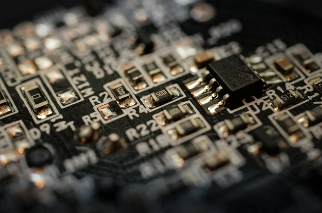
A Package Test PCB is a specialized semiconductor test PCB used to validate IC packages after wafer dicing and packaging. These PCBs provide reliable electrical and mechanical interfaces for Automated Test Equipment (ATE), ensuring that packaged ICs meet functional, parametric, and performance specifications.
With modern ICs moving toward higher pin counts, fine pitch packages, and high-speed operation, package test PCBs must maintain signal integrity, mechanical precision, and robust reliability to guarantee accurate testing results.
Key Design Features of Package Test PCBs
1. High Pin Count and Dense Interconnects
Modern IC packages often feature hundreds to thousands of pins, requiring HDI PCB technology, fine-line routing, and multilayer stackups to handle dense signal routing while maintaining signal fidelity.
2. Controlled Impedance and Signal Integrity
To accurately test high-speed ICs, package test PCBs must ensure precise controlled impedance, matched trace lengths, and minimal crosstalk, maintaining high signal quality across all channels.
3. Mechanical Accuracy and Reliability
Package test PCBs require precise pad alignment, flatness, and dimensional stability to ensure reliable contact with test sockets and ATE connectors during repeated testing cycles.
4. Robust Power and Ground Design
Optimized power distribution networks, decoupling, and low-impedance ground planes deliver stable power to the IC, minimizing noise and voltage fluctuations during high-speed functional tests.
5. Thermal Stability and Material Selection
High-Tg, low-loss laminates enable the PCB to withstand thermal cycling and extended testing durations, ensuring consistent electrical performance and long-term reliability.
Applications of Package Test PCBs
Package test PCBs are widely used in:
-
Memory and DRAM/Flash package testing
-
Logic IC and microprocessor package validation
-
Mixed-signal and RF IC package evaluation
-
Automotive and industrial semiconductor package testing
-
High-reliability IC package qualification
These applications demand accuracy, repeatability, and robust electrical performance.
Manufacturing Requirements for Package Test PCBs
High-quality package test PCBs require:
-
Multilayer and HDI PCB fabrication
-
Fine-line etching and microvia technology
-
Controlled impedance verification and high-density routing
-
Precision lamination and flatness control
-
Prototype, small batch, and volume production support
Advanced manufacturing ensures stable signal integrity, mechanical reliability, and long-term performance for complex IC package testing.
Why Package Test PCB Quality Matters
Low-quality package test PCBs can lead to:
-
Unstable or incomplete pin contact
-
Signal degradation and measurement errors
-
Increased ATE equipment downtime
-
Reduced test yield and higher operational costs
High-quality Package Test PCBs guarantee accurate IC package testing, repeatable results, and optimal production efficiency.
Conclusion
The Package Test PCB is a fundamental component in IC package validation, providing precise electrical routing, controlled impedance, and mechanical stability for high-pin-count, fine-pitch IC packages. With advanced HDI layouts, multilayer construction, and premium materials, package test PCBs enable reliable and repeatable testing across high-speed, mixed-signal, and high-density IC applications.
Collaborating with a professional package test PCB manufacturer ensures accurate testing, improved yield, and long-term reliability in demanding ATE environments.
