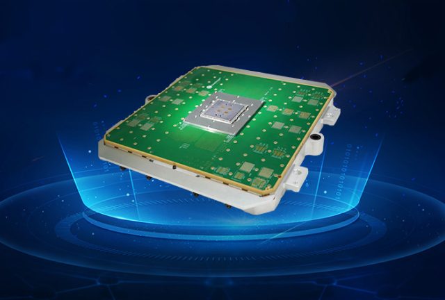
A Probe Card Assembly PCB is a critical semiconductor test PCB used in wafer-level testing to provide the electrical and mechanical interface between Automated Test Equipment (ATE) and semiconductor wafers. It supports probe needles or MEMS probes, routing test signals with extreme precision to ensure accurate electrical characterization before wafer dicing and packaging.
As semiconductor devices continue to scale toward higher pin counts, finer pitches, and higher operating frequencies, probe card assembly PCBs must deliver outstanding signal integrity, mechanical accuracy, and long-term reliability.
Core Design Requirements of Probe Card Assembly PCBs
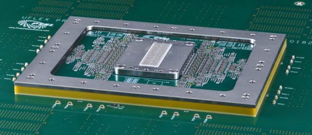
1. Ultra-Fine Pitch and High Pin Count Routing
Probe card assembly PCBs support thousands of probe contacts in very limited space. This requires HDI PCB technology, microvias, ultra-fine trace widths, and multilayer stackups to achieve reliable fanout without signal degradation.
2. Controlled Impedance and Signal Integrity
High-speed and RF wafer testing demands precise controlled impedance routing, tight trace length matching, and minimized parasitic effects to ensure accurate measurement of IC performance parameters.
3. Exceptional Mechanical Precision
Probe card assembly PCBs must maintain excellent flatness, dimensional stability, and pad accuracy to guarantee consistent probe contact across the entire wafer surface, even under repeated testing cycles.
4. Robust Power and Ground Architecture
Stable power delivery is essential for wafer-level testing. Optimized power distribution networks (PDN) and low-impedance ground planes help reduce noise and voltage fluctuation during high-speed testing.
5. Thermal Stability and Reliability
Probe card assembly PCBs must withstand thermal cycling and long test durations. High-Tg materials and robust multilayer construction ensure consistent performance over extended operational lifetimes.
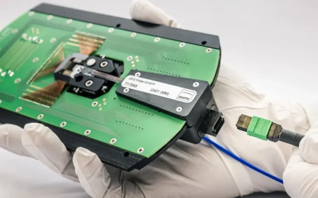
Applications of Probe Card Assembly PCBs
Probe card assembly PCBs are widely used in:
-
Wafer-level logic IC testing
-
Memory and storage semiconductor probing
-
RF and mmWave wafer testing
-
Automotive and high-reliability semiconductor qualification
-
Advanced node and high-density IC validation
These applications require extreme accuracy, repeatability, and durability from the probe card PCB.
Manufacturing Capabilities for Probe Card Assembly PCBs
Producing high-quality probe card assembly PCBs requires advanced fabrication processes, including:
-
HDI and multilayer PCB manufacturing
-
Ultra-fine line etching and precision drilling
-
Microvia and blind/buried via technology
-
Controlled impedance testing and verification
-
Tight tolerance lamination and flatness control
Precision manufacturing ensures consistent electrical performance and long probe card service life.
Why Probe Card Assembly PCB Quality Matters
Low-quality probe card assembly PCBs can lead to:
-
Inconsistent probe contact and unstable signals
-
Measurement errors and reduced test accuracy
-
Increased probe wear and equipment downtime
-
Lower wafer yield and higher production costs
A high-quality probe card assembly PCB ensures accurate wafer-level testing, stable electrical performance, and long-term reliability.
Conclusion
The Probe Card Assembly PCB is the foundation of wafer-level semiconductor testing, enabling precise electrical contact and accurate signal routing between ATE systems and semiconductor wafers. Through HDI design, controlled impedance routing, and precision manufacturing, probe card assembly PCBs support reliable testing for advanced IC technologies.
Partnering with an experienced probe card assembly PCB manufacturer ensures high test accuracy, improved yield, and long-term stability in demanding semiconductor test environments.
