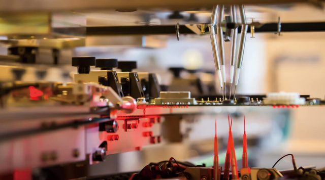
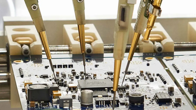
An Automated Test Equipment PCB (ATE PCB) is a critical component used in semiconductor testing systems to interface between the test equipment and the device under test (DUT). These PCBs enable precise electrical connections, accurate signal transmission, and stable power delivery required for validating IC functionality, performance, and reliability.
As semiconductor devices continue to evolve toward higher speeds, higher pin counts, and greater integration, automated test equipment PCBs must meet increasingly strict requirements for signal integrity, power integrity, and mechanical stability.
Key Design Requirements of Automated Test Equipment PCBs
1. High Pin Count and Dense Interconnects
ATE PCBs often support devices with hundreds or thousands of I/O pins. This requires high-density routing, multilayer stackups, and HDI technology to ensure efficient fanout while maintaining electrical performance.
2. Controlled Impedance and Signal Integrity
High-speed digital, analog, and RF testing demands strict controlled impedance, precise trace length matching, and minimized crosstalk. Proper stackup design is essential to maintain signal accuracy across all test channels.
3. Robust Power Integrity Design
Automated test equipment PCBs must deliver stable power under dynamic load conditions. Optimized power distribution networks (PDN), solid ground planes, and effective decoupling strategies reduce noise and voltage fluctuation during testing.
4. Mechanical Precision and Reliability
ATE PCBs must maintain excellent flatness, dimensional accuracy, and mechanical strength to ensure reliable connections with test sockets, probe cards, and connectors across repeated test cycles.
5. Thermal Stability and Durability
Long test cycles and high-power devices require ATE PCBs to withstand thermal stress. High-Tg materials and robust construction ensure long-term reliability and consistent test results.
Applications of Automated Test Equipment PCBs
Automated test equipment PCBs are widely used in:
-
Logic and processor IC testing
-
Memory and storage device testing
-
RF and microwave semiconductor testing
-
Automotive and industrial IC validation
-
High-reliability and aerospace semiconductor testing
These applications require high accuracy, repeatability, and durability from the ATE PCB.
Manufacturing Capabilities for ATE PCBs
Producing reliable automated test equipment PCBs requires advanced manufacturing processes, including:
-
Multilayer and HDI PCB fabrication
-
Fine-line etching and precision drilling
-
Controlled impedance verification
-
High pin count and tight tolerance processing
-
Prototype, small batch, and volume production support
Precision manufacturing ensures consistent electrical performance and long service life.
Why Automated Test Equipment PCB Quality Matters
Poor-quality ATE PCBs can result in:
-
Inconsistent electrical contact and signal degradation
-
Inaccurate test results and false failures
-
Increased equipment downtime and maintenance costs
-
Reduced semiconductor test yield
High-quality automated test equipment PCBs ensure accurate, repeatable, and efficient semiconductor testing, improving overall production efficiency.
Conclusion
The Automated Test Equipment PCB is the foundation of modern semiconductor testing systems, enabling precise electrical connections, controlled impedance routing, and stable power delivery. Through advanced design, high-quality materials, and precision manufacturing, ATE PCBs support reliable testing for high-speed, high-pin-count, and high-frequency semiconductor devices.
Choosing an experienced automated test equipment PCB manufacturer ensures consistent test accuracy, reduced downtime, and long-term system reliability for advanced semiconductor testing applications.
