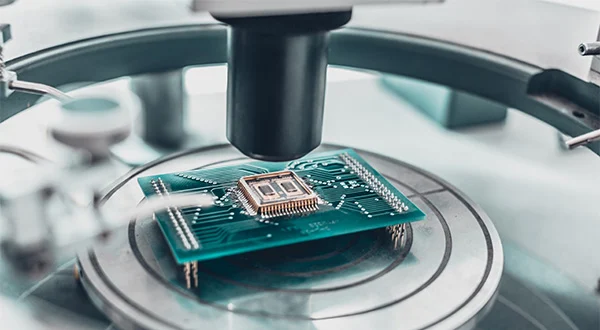
A Package Test PCB is a critical component in Automated Test Equipment (ATE) setups, designed to test ICs at the package level after assembly. These PCBs serve as the interface between test sockets or probe systems and the semiconductor device, ensuring high-precision electrical contact, stable signal transmission, and repeatable testing.
With modern ICs moving toward smaller package sizes, higher pin counts, and mixed-signal or high-speed designs, package test PCBs must deliver exceptional signal integrity, mechanical stability, and manufacturing precision to support reliable testing.
Core Features of Package Test PCBs
1. High Pin Count and Dense Routing
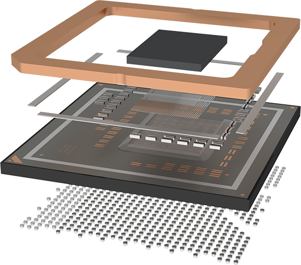
Package test PCBs support IC packages such as BGA, QFN, LGA, CSP, and SiP. High pin density requires HDI multilayer designs, microvias, and fine-line routing to maintain signal integrity and fanout capabilities.
2. Controlled Impedance for High-Speed Signals
High-speed IC packages demand precise impedance control, trace matching, and crosstalk suppression. Proper stackup design ensures consistent electrical performance across all channels.
3. Mechanical Precision and Socket Compatibility
Accurate pad layout, PCB flatness, and dimensional stability are crucial to maintain reliable contact with sockets and probe pins, especially in repeated insertion and removal cycles.
4. Robust Power and Ground Integrity
Optimized power distribution networks (PDN), decoupling strategies, and ground plane design reduce noise and voltage fluctuation, ensuring precise parametric testing for analog, digital, and RF IC packages.
5. Thermal and Reliability Considerations
Package test PCBs must withstand repeated thermal cycling and test stress. High-Tg and low-loss materials are commonly used to maintain long-term electrical and mechanical stability.
Applications of Package Test PCBs
Package test PCBs are widely used in:
-
Logic and microprocessor IC package testing
-
Memory and storage device validation
-
RF, mmWave, and mixed-signal IC evaluation
-
Automotive and industrial IC quality testing
-
High-reliability and aerospace semiconductor applications
Each application relies on stable probe contact, repeatable measurements, and low insertion loss.
Manufacturing Requirements for Package Test PCBs
High-performance package test PCBs demand:
-
HDI multilayer PCB fabrication with microvias and blind/buried vias
-
Fine-line and fine-pitch etching for dense pin layouts
-
Controlled impedance verification
-
High-Tg, low-loss laminate processing
-
Prototype, small batch, and volume production support
Advanced manufacturing ensures signal integrity, mechanical reliability, and repeatable testing.
Why Package Test PCB Quality Is Critical
Inferior package test PCBs can lead to:
-
Inconsistent probe contact and signal loss
-
Reduced measurement accuracy
-
Increased ATE downtime and socket wear
-
Lower semiconductor test yields
High-quality package test PCBs deliver accurate, reliable, and repeatable test results, ensuring ICs meet stringent electrical and mechanical specifications.
Conclusion
The Package Test PCB is a cornerstone of IC package validation and semiconductor testing, providing high-density routing, controlled impedance, and robust mechanical design for precise probe or socket testing. Partnering with an experienced package test PCB manufacturer ensures high accuracy, repeatable results, and efficient ATE operation, supporting advanced ICs in automotive, high-speed, RF, and mixed-signal applications.
